Open drain driver, and a switch comprising the open drain driver

a technology of open drain and driver, which is applied in the direction of electronic switching, pulse technique, instruments, etc., can solve the problems of single fet failing as a result of over-voltage, single fet suffering from serious disadvantage of open drain driver, etc., to improve over-voltage protection, enhance over-voltage protection, and minimise the vulnerability of open drain driver

Active Publication Date: 2008-09-23
ANALOG DEVICES INC
View PDF16 Cites 12 Cited by
  • Summary
  • Abstract
  • Description
  • Claims
  • Application Information

AI Technical Summary

Benefits of technology

[0074]The advantages of the open drain driver according to the invention are many. The open drain driver according to the invention is reliable and robust, and is suitable for implementing in low supply voltage rated CMOS environments, and is particularly suitable for use in applying one of the logic high and logic low states to a gate of a transistor switch, which is passively held in the other of the logic high and logic low states. Since the open drain driver according to the invention is provided with improved over-voltage protection, it is particularly suitable for applying one of the logic low and the logic high states to a gate of a transistor switch, which is passively held in the other of the logic high and logic low states, where such a transistor switch is switching high frequency AC analogue input signals, and in particular, analogue video signals of frequency in the range 27 MHz to 81 MHz, and where the AC signal is capacitively coupled to the gate of the transistor switch, in order to remove variability of the on-resistance of the transistor switch to reduce distortion in the signal being switched by the transistor switch.
[0075]Firstly, by virtue of the fact that the open drain driver according to the invention comprises first and second transistors, any over-voltage which is applied to the output of the open drain driver is divided across the first and second transistors, thus minimising the vulnerability of the open drain driver to over-voltages applied to its output node. Secondly, the provision of the coupling element which couples the coupling node to a reference voltage node for limiting the voltage on the coupling node further enhances the over-voltage protection provided in the open drain driver, since by limiting the voltage on the coupling node, the voltage to which the second transistor can be subjected is likewise limited, and can be limited to a value which does not exceed the permitted reliability limit of the second transistor. Accordingly, any danger of the voltage on the coupling node rising or falling, depending on whether the first and second transistors are N-type or P-type transistors as a result of DC currents leaking through the first transistor, or AC currents being capacitively coupled through the first transistor, when the first and second transistors are in the non-conducting state is avoided.
[0076]Where the coupling element is provided by a DC coupling element implemented, for example, by a diode, the DC voltage on the coupling node is maintained at a voltage which does not rise above or fall below the reference voltage which is applied to the reference voltage node by the value of the conducting voltage of the diode, depending on whether the first and second transistors are N-type or P-type transistors. By capacitively coupling the coupling node to the reference voltage node, or any other low impedance node, the voltage, resulting from capacitive coupling of the coupling node to the output node through the parasitic capacitance of the first transistor, to which the coupling node can rise or fall, depending on the type of circuit, is limited by the attenuating effect of the coupling capacitor. The attenuation of the voltage capacitively coupled to the coupling node from the output node is a function of the ratio of the parasitic capacitance of the first transistor coupling the coupling node to the output node to the sum of the capacitance of the coupling capacitor and the parasitic capacitances of the first and second transistors which couple the coupling node to low impedance nodes. Accordingly, by appropriately selecting the value of the capacitance of the coupling capacitor, the voltage on the coupling node can be limited to avoid the voltage capacitively coupled to the coupling node from the output node rising to or falling to a voltage which would cause failure of the second transistor, depending on whether the first and second transistors are N-type or P-type transistors.
[0077]Capacitive coupling of the coupling node to the reference voltage node or to any other low impedance node provides the advantage that the open drain driver is particularly suitable for use in high frequency AC analogue signal environments. Additionally, the capacitive coupling of the coupling node to the reference voltage node or to any other low impedance node for limiting the voltage capacitively coupled to the coupling node provides the advantage that the open drain driver according to the invention is particularly suitable for low voltage environments, and in particular, for low voltage CMOS environments of rated supply voltages of 3.3 volts, such as CMOS circuits implemented in 0.18 micron CMOS processes, and CMOS circuits with even lower rated supply voltages, such as rated supply voltages as low as one volt.
[0078]Additionally, when the open drain driver is used in conjunction with a passively operated transistor switch, in particular, a passively operated MOSFET switch, the open drain driver has the added advantage that when the switch is passively held in an open state, the open drain driver presents a high impedance to the gate of the MOSFET switch, and thus, the open drain driver has little or no effect on the signal being switched by the MOSFET switch. In particular, when the signal being switched by the MOSFET switch is a high frequency analogue AC signal, such as, for example, an analogue video signal at a frequency in the range of 27 MHz to 81 MHz, the signal can be switched with virtually no distortion so that the output signal from the MOSFET switch corresponds to the input signal without distortion. Additionally, by virtue of the fact that the value to which the voltage on the coupling node between the first and second transistors of the open drain driver can rise is limited by virtue of the provision of the coupling element coupling the coupling node to the reference voltage node, and where the coupling element is a capacitive coupling element, coupling the coupling node to any low impedance node, the open drain driver has significantly improved protection against over-voltages which result from the AC signal being switched by the MOSFET, than open drain drivers known heretofore.
[0073]In one embodiment of the invention the coupling node is capacitively coupled to the at least one low impedance node through a capacitive coupling element, and additionally or alternatively, the second transistor is sized relative to the first transistor to provide the capacitive coupling of the coupling node to the at least one low impedance node, and the at least one low impedance node is the switching voltage node and is provided as a low impedance node.
[0080]The provision of the switch circuit according to the invention incorporating the open drain driver provides a switch circuit which is particularly suitable for switching analogue AC signals, since the open drain driver is provided with improved over-voltage protection.

Problems solved by technology

This, in turn, would lead to failure of such an open drain driver.
Open drain drivers which comprise a single FET suffer from a serious disadvantage when operating in low supply voltage rated environments, in particular, in CMOS environments, which are designed to operate at rated supply voltages of the order of 5 volts, and in many cases at rated supply voltages of the order of 3.3 volts, and in some cases, at rated supply voltages as low as 1 volt.
Similarly, in a case where an open drain driver is used to apply the one of a logic high or a logic low state to the gate of a transistor switch, if the gate of the transistor switch is subjected to a voltage higher than the rated supply voltage plus 10% of the single FET of the open drain driver, the single FET will fail as a result of the over-voltage.
In CMOS applications where a MOSFET switch is switching an AC signal, linearity problems arise in the MOSFET switch.
Thus, as the voltage of the AC signal on the drain-source of the MOSFET switch varies from peak to peak, the voltage across the gate and drain and the gate and source of the MOSFET switch also varies, thereby varying the on-resistance of the MOSFET switch and in turn compromising the linearity of the AC signal switched through the MOSFET switch.
However, if such an AC coupled MOSFET switch were passively held in the conducting state and held in the non-conducting state by a logic signal applied to the gate through an open drain driver, the open drain driver would be subjected to the AC voltage which is AC coupled to the gate of the MOSFET switch, and this could result in an over-voltage being applied to the open drain driver when the open drain driver is in the high impedance state, which in turn would lead to failure of the open drain driver.
However, a problem with the open drain driver of Wei is that the voltage on a node through which the source of the first MOSFET is coupled to the drain of the second MOSFET can increase to a level which exceeds the permitted reliability voltage limit of the second MOSFET, and in certain cases, the first MOSFET.
This thus leads to failure of the second MOSFET.

Method used


Image

  • Open drain driver, and a switch comprising the open drain driver
  • Open drain driver, and a switch comprising the open drain driver
  • Open drain driver, and a switch comprising the open drain driver

Examples


Embodiment Construction

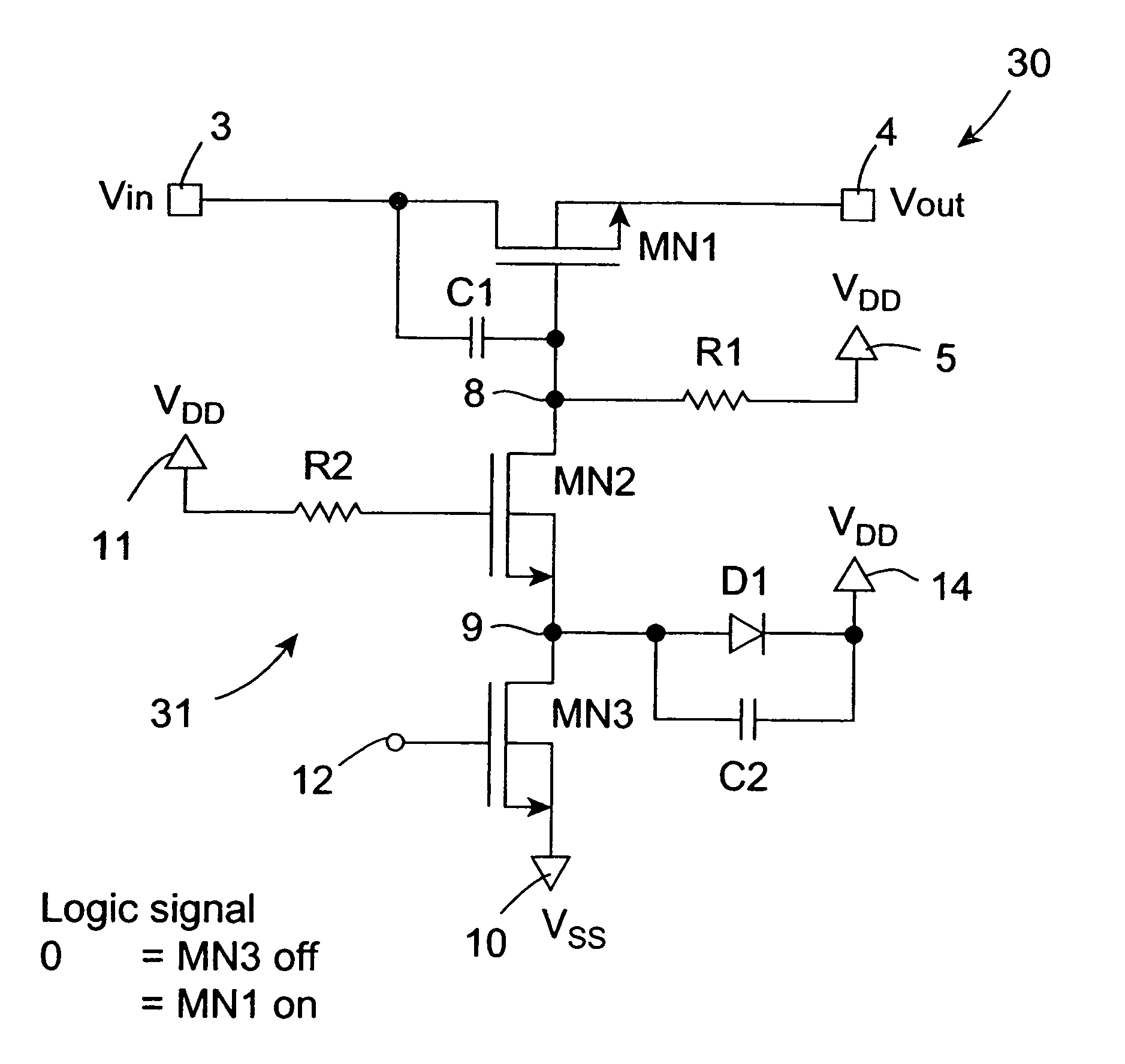
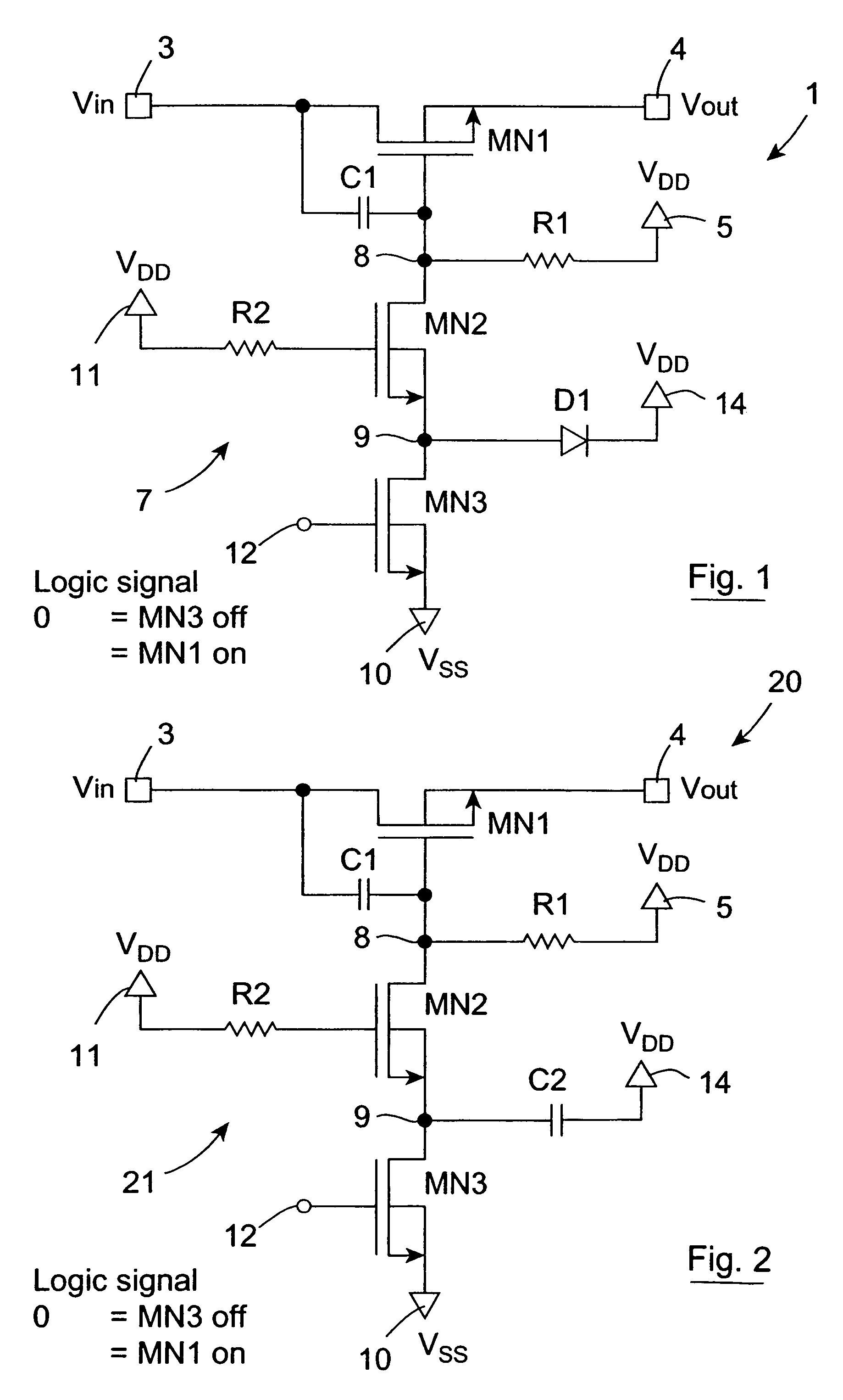
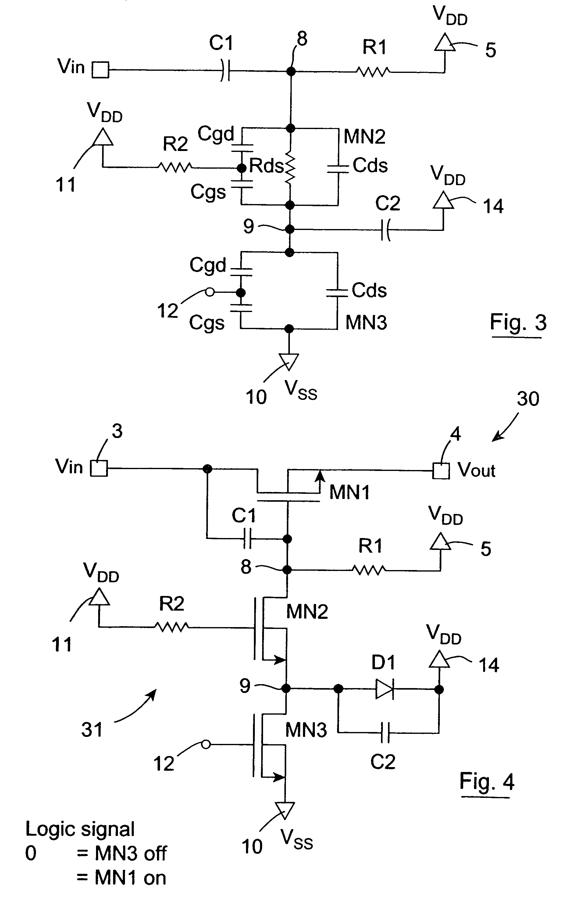
[0090]Referring to the drawings and initially to FIG. 1, there is illustrated a switch circuit according to the invention, indicated generally by the reference numeral 1 for selectively switching an input signal Vin. In this case the switch circuit 1 is implemented as a low voltage CMOS integrated circuit, and is particularly suitable for switching a high frequency analogue AC input signal Vin, for example, an analogue video signal of frequency in the range of 27 MHz to 81 MHz, although needless to say, the switch circuit 1 is suitable for switching any type of signal, both AC and DC.

[0091]The switch circuit 1 comprises a main input terminal 3 to which the input signal Vin is applied, and a main output terminal 4 to which the input signal Vin is switched and appears as Vout. A transistor switch provided by an N-channel MOSFET switch MN1 located between the main input terminal 3 and the main output terminal 4 selectively switches the input signal Vin to the main output terminal 4. In...


PUM


Abstract

An open drain driver (7) selectively switches a MOSFET switch (MN1) which is passively held in the conducting state into the non-conducting state. The MOSFET switch (MN1) switches an AC analogue input signal on a main input terminal (3) to a main output terminal (4) and the gate of the MOSFET switch (MN1) is AC coupled by a capacitor (C1) to the drain thereof. The open drain driver (7) comprises a first MOSFET (MN2) and a second MOSFET (MN3) through which the gate of the MOSFET switch (MN1) is pulled to ground (Vss). The gate of the first MOSFET (MN2) is coupled to the supply voltage (VDD) for maintaining the first MOSFET (MN2) in the open state. A control signal is applied to the gate of the second MOSFET (MN3) for selectively operating the open drain driver (7) in the conducting state for operating the MOSFET switch (MN1) in the non-conducting state. When the second MOSFET (MN3) is in the non-conducting state, the first MOSFET (MN2) remains in the conducting state until the voltage on a coupling node (9) between the first and second MOSFETs (MN2,MN3) equals the difference between its gate voltage and its threshold voltage, at which stage, any over-voltages applied to the gate of the MOSFET switch (MN1) are divided between the first and second MOSFETs (MN2,MN3). A coupling diode (D1) coupling the coupling node (9) to the supply voltage (VDD) clamps the voltage on the coupling node (9) at the supply voltage (VDD) plus the conducting voltage of the diode (D1), in the event of the voltage on the coupling node (9) rising after the first MOSFET (MN2) has gone into the non-conducting state. The coupling node (9) may be capacitively coupled to the supply voltage (VDD) by a coupling capacitor instead of or as well as the diode (D1) for limiting the voltage on the coupling node (9).

Description

FIELD OF THE INVENTION[0001]The present invention relates to an open drain driver, and a switch circuit comprising a transistor switch operating under the control of an open drain driver. The invention also relates to a method for providing an open drain driver with improved over-voltage breakdown protection.BACKGROUND TO THE INVENTION[0002]Open drain drivers are well known, and have many applications. For example, open drain drivers are commonly used for driving a low signal from an associated circuit onto a shared bus to a remote external circuit. The advantage of using an open drain driver in such an application is that when the open drain driver is not required to drive the low signal onto the shared bus, the open drain driver is in a high impedance state, thereby isolating its associated circuit from the shared bus. In such cases, where a plurality of circuits are sharing a bus, the rated supply voltages of the circuits may vary depending on the type of circuit. Some circuits m...

Claims


Application Information

Patent Timeline
Patent Type & Authority Patents(United States)
IPC IPC(8): H03K17/687
CPCH03K17/063H03K17/6872H03K17/102H03K17/08142
Inventor O'DONNELL, JOHN J.COLN, MICHAEL CHRISTIAN WOHNSENMARTI, MARIA DEL MAR CHAMARRO
Owner ANALOG DEVICES INC
Why Eureka
Try Eureka