
High read output, high sensitivity magnetic sensing element

a high-sensitivity, magnetic sensing element technology, applied in the field of magnetic sensing elements, can solve the problems of degradation of read characteristics, limited area of composite surface, increased gap length, etc., and achieve the effect of easy optimization of the distance between the free magnetic layer and the antiferromagnetic layer for controlling the magnetization direction of the free magnetic layer

Inactive Publication Date: 2008-09-23
TDK CORPARATION
View PDF19 Cites 7 Cited by
  • Summary
  • Abstract
  • Description
  • Claims
  • Application Information

AI Technical Summary

Benefits of technology

[0015]The present invention aims to overcome the above-described problems of the conventional art. An object of the present invention is to provide a practicable high read output, high sensitivity magnetic sensing element having pinned magnetic layer arranged at the two sides of a free magnetic layer in the track width direction, in which an electric current flows through these layers.
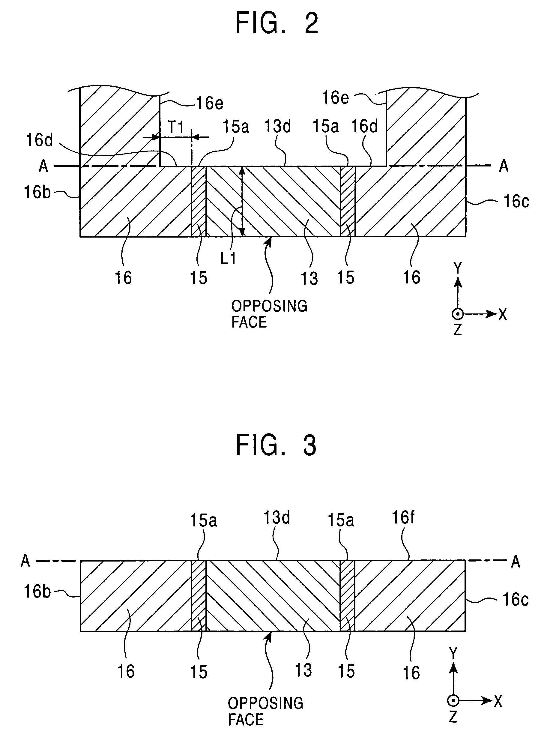
[0020]In each of the magnetic sensing elements described above the regions of the pinned magnetic layers near the free magnetic layer are narrowed to increase the current density. According to this structure, read output can be improved.
[0023]According to the structure in which the specular layer is formed under the free magnetic layer and / or the pinned magnetic layers, conduction electrons having a spin with a longer mean free path (majority electrons), e.g., spin-up conduction electrons, undergo diffusive scattering at the top face or the bottom face of the free magnetic layer if the thickness of the free magnetic layer is excessively small. This results in shorter spin diffusion lengths and degradation of the change in resistance ΔR. Thus, the thickness of the free magnetic layer is sufficiently large. However, at an excessively large thickness, the magnetic moment of the free magnetic layer per unit area (hereinafter, simply referred to as “Ms·t”, since the magnetic moment is the product of the saturation magnetization Ms and the thickness t) becomes excessively large, and the read sensitivity is degraded as a result. By providing the specular layer, the spin diffusion length can be extended without excessively increasing the thickness of the free magnetic layer, and a magnetic sensing element having superior MR characteristics can be obtained. Moreover, the thickness of the pinned magnetic layers does not have to be large when the specular layers are provided. Thus, an exchange coupling magnetic field of an appropriate intensity can be generated between the pinned magnetic layers and the antiferromagnetic layers.
[0029]In order to overcome this problem, the free magnetic layer is provided as a composite of magnetic sublayers and nonmagnetic interlayers, and the magnetization directions of all of the magnetic sublayers are oriented in the same direction. When the free magnetic layer has such a multilayer structure, the specular layer may or may not be used. In this manner, conduction electrons having a spin with a shorter mean free path, e.g., spin-down conduction electrons, can be easily scattered at the interfaces between the magnetic sublayers and the nonmagnetic interlayers (the spin filtering effect). Meanwhile, conduction electrons having a spin with a longer mean free path, e.g., spin-up conduction electrons (majority electrons), are not scattered inside the free magnetic layer or at the interfaces between the nonmagnetic interlayers and the magnetic sublayers. As a result, the same advantage as those achieved by increasing the thickness of the free magnetic layer, i.e., extended spin diffusion length, can be achieved. Moreover, the difference in the mean free path between the conduction electrons having a spin with a longer mean free path and those with a shorter mean free path can be widened. As a result, the change in resistance ΔR can be increased, and the read output can be improved.
[0030]Furthermore, when the free magnetic layer has the multilayer structure, the thickness of the free magnetic layer can be increased while decreasing the volume ratio of the magnetic sublayers to the entire volume of the free magnetic layer. In this manner, the effective Ms·t can be decreased, and the read sensitivity can be improved. The magnetic sublayers are ferromagnetically coupled with each other through RKKY coupling, direct exchange coupling via pinholes, or topological coupling, so that the multilayer structure as a whole can behave as if it is an integral ferromagnetic member.
[0033]A third aspect of the present invention provides a magnetic sensing element including a composite that includes a free magnetic layer; nonmagnetic conductive layers; and pinned magnetic layers, in which an antiferromagnetic layer is provided above or under the free magnetic layer so as to control the magnetization direction of the free magnetic layer. In this embodiment, antiferromagnetic layers for pinning the magnetization directions of the pinned magnetic layers are no longer necessary. Moreover, the distance between the free magnetic layer and the antiferromagnetic layer for controlling the magnetization direction of the free magnetic layer can be easily optimized. Thus, the free magnetic layer can be easily put to a single-magnetic-domain state.

Problems solved by technology

The extent to which the area of the surface of the composite can be decreased is limited according to the current photolithographic technology.
Moreover, increasing the thickness of the composite results in an increase in the gap length, which results in degradation of the read characteristics.
However, these publications do not sufficiently provide substantial means for putting these magnetic sensing elements into actual application.
None of the above-described publications provide sufficient disclosure regarding this point.
In general, TMR elements already have high element resistance; hence, when the structure disclosed in this publication is employed, the resistance will further increase since the area of the cross-section taken in the direction of current flow is decreased, thereby making the practical application more difficult.

Method used


Image

  • High read output, high sensitivity magnetic sensing element
  • High read output, high sensitivity magnetic sensing element
  • High read output, high sensitivity magnetic sensing element

Examples


Embodiment Construction

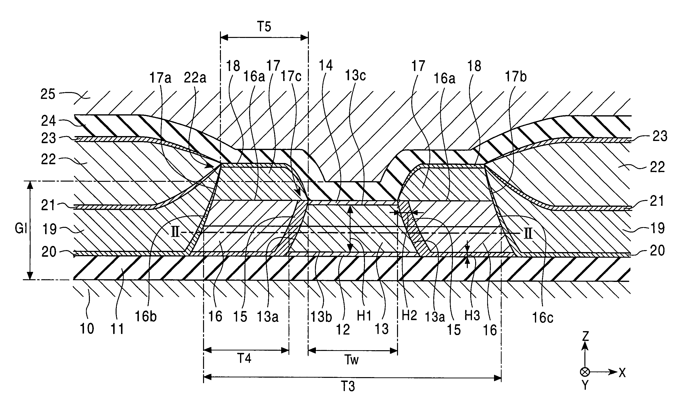
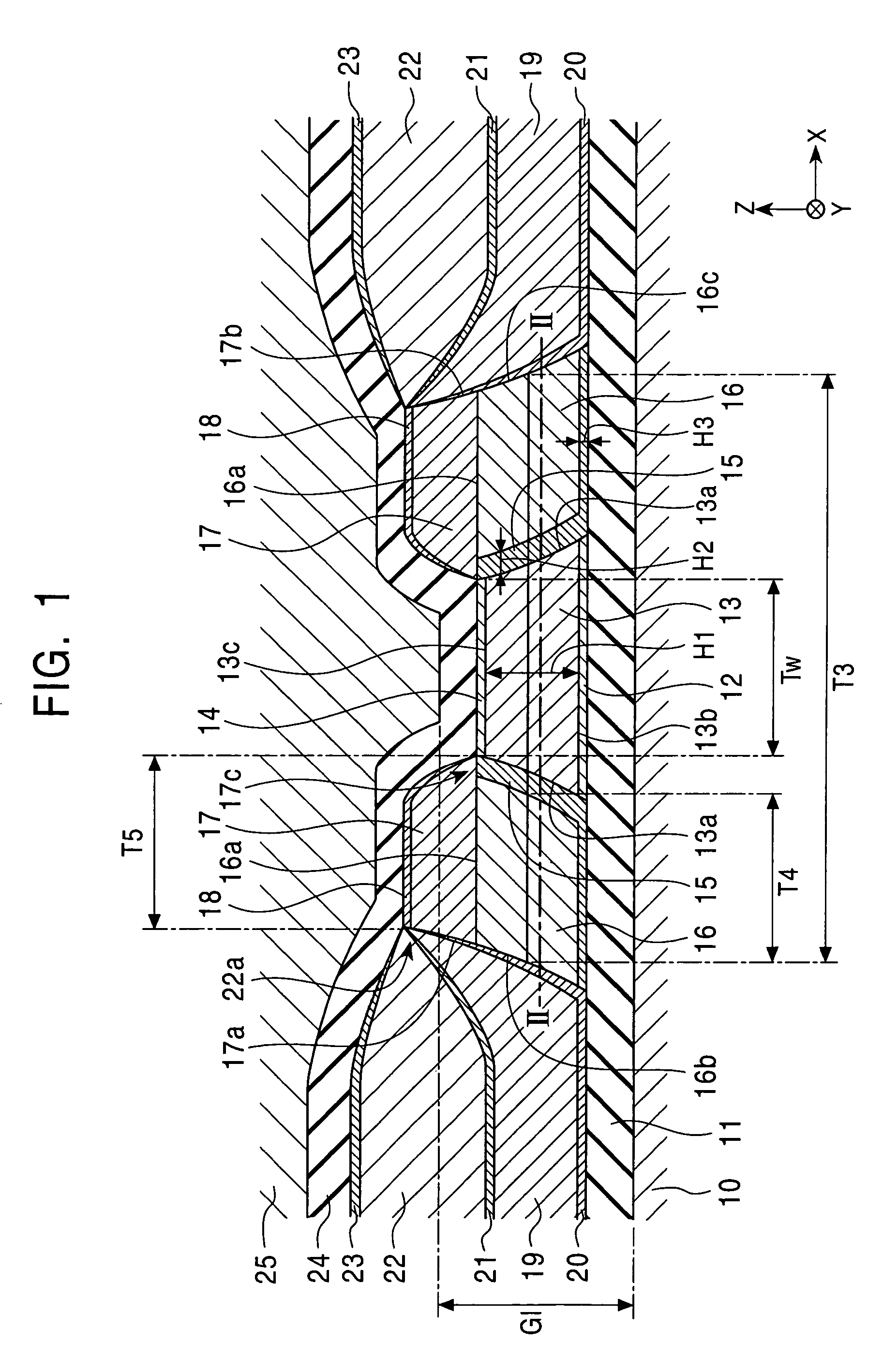
[0045]FIG. 1 is a cross-sectional view of a magnetic sensing element according to a first embodiment of the present invention viewed from a face of the magnetic sensing element opposing a recording medium (hereinafter, this face is referred to as the “opposing face”). The cross-sectional view is taken parallel to the opposing face.

[0046]The magnetic sensing element shown in FIG. 1 is a giant magnetoresistive (GMR) head for reading an external signal recorded on a recording medium. An inductive writing head may be disposed on the magnetic sensing element, although this is not shown in the drawing.

[0047]In the following description, surfaces of the layers constituting the magnetic sensing element lie in the X-Y plane as defined in each of the drawings. The term “track width direction” refers to a direction parallel to the X direction. The width of a region having magnetization that changes in response to an external magnetic field coincides with this “track width direction”. For examp...


PUM


Abstract

A magnetic sensing element has pinned magnetic layers disposed on the two sides of a free magnetic layer in the track width direction with nonmagnetic conductive layers therebetween, and an electric current flows through these layers in parallel to the surfaces. The back end of the free magnetic layer in the track width direction extends in parallel to the track width direction. The back ends of the nonmagnetic conductive layers are coincident with the reference line drawn by extending the back end of the free magnetic layer. At least part of the back ends of the pinned magnetic layers is coincident with the reference line. Each pinned magnetic layer is shaped so that the region near the nonmagnetic conductive layer and the free magnetic layer has a smaller length in the height direction to achieve higher current density.

Description

[0001]This application claims the benefit of priority to Japanese Patent Application No. 2003-006625, herein incorporated by reference.BACKGROUND OF THE INVENTION[0002]1. Field of the Invention[0003]The present invention relates to a magnetic sensing element in which pinned magnetic layers are disposed at the two sides of the free magnetic layer in the track width direction, in which electric current flows parallel to the surfaces of these layers. In particular, it relates to a magnetic sensing element having improved read outputs and superior sensitivity.[0004]2. Description of the Related Art[0005]A magnetic sensing element constituted from a composite including a free magnetic layer, a nonmagnetic conductive layer, a pinned magnetic layer, and an antiferromagnetic layer stacked in the film thickness direction, in which electric current flows perpendicular to the surface of each layer of the composite, is called current-perpendicular-to-the-plane (CPP) magnetic sensing element. St...

Claims


Application Information

Patent Timeline
IPC IPC(8): G11B5/39H01L43/00H01F10/16H01F10/32H01L43/08H01L43/10
CPCG11B5/3906
Inventor HASEGAWA, NAOYASAITO, MASAMICHI
Owner TDK CORPARATION
Learn More