
Compositions for dissolution of low-k dielectric film, and methods of use

a dielectric film and composition technology, applied in the field of compositions for dissolving low-k dielectric films, can solve the problems of gummy organic residues on the surface of wafers, wet hf chemistries having difficulty removing low-k dielectric films such as tms-based low-k dielectric films, and inorganic non-surface active detergent compositions

Inactive Publication Date: 2008-10-07
MICRON TECH INC
View PDF89 Cites 1 Cited by
  • Summary
  • Abstract
  • Description
  • Claims
  • Application Information

AI Technical Summary

Benefits of technology

The solution enables efficient and controlled removal of low-k dielectric and photoresist layers, producing a hydrophobic surface, with removal rates adjustable from 50 to 1000 angstroms per minute, effectively addressing the limitations of existing methods by maintaining the integrity of underlying silicon surfaces.

Problems solved by technology

Since many tests are destructive or will harm the product wafer, the measurements are typically performed on a test or “dummy” wafer, which are blank wafers that are mixed in with the product wafers.
Since silicon wafers are expensive, when the processing and testing is completed, the dummy wafers are usually cleaned, inspected, and reused.
However, wet HF chemistries have difficulty removing low-k dielectrics such as a TMS-based low-k dielectric film, largely due to organic components in the oxide films.
As a result, cleaning with an HF solution can leave the wafer with a gummy organic residue on the surface.

Method used


Image

  • Compositions for dissolution of low-k dielectric film, and methods of use
  • Compositions for dissolution of low-k dielectric film, and methods of use
  • Compositions for dissolution of low-k dielectric film, and methods of use

Examples


example

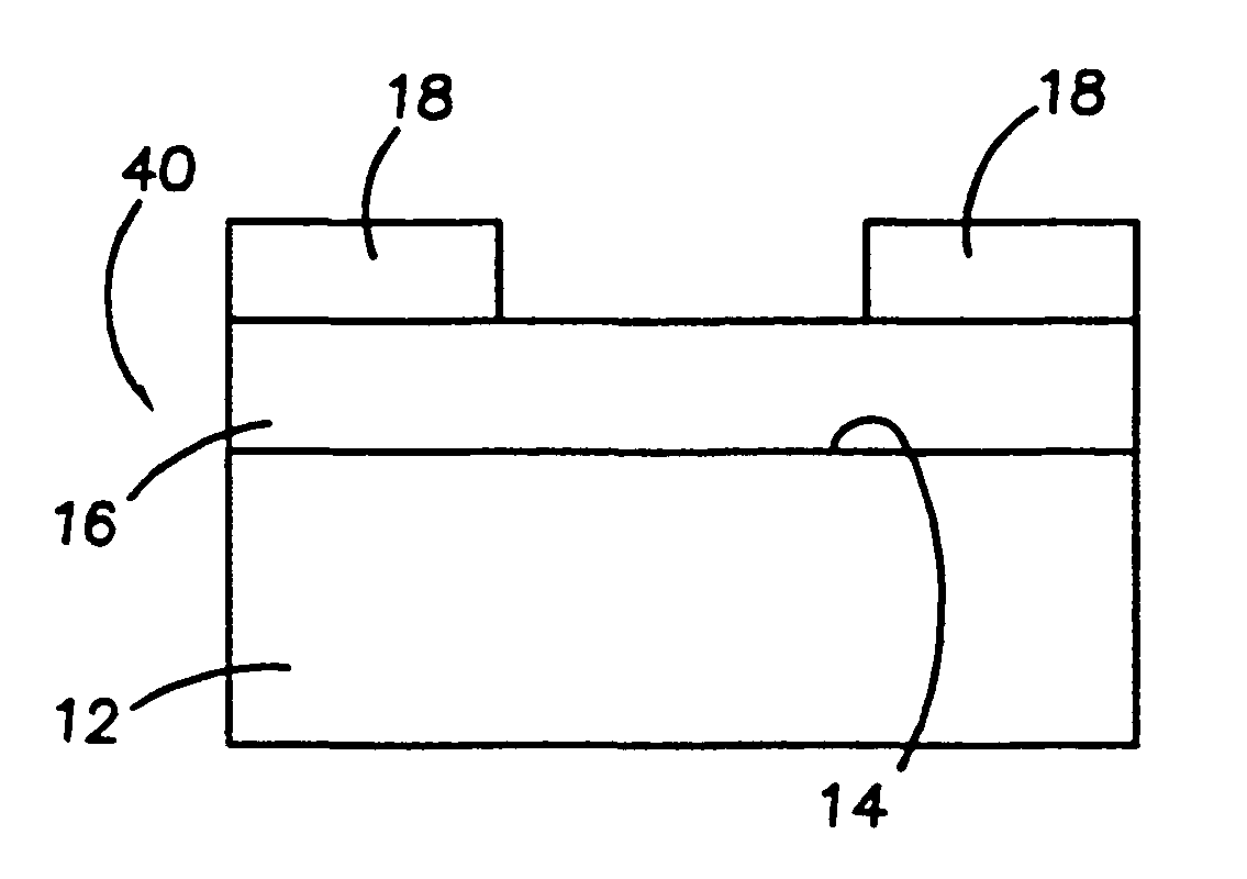
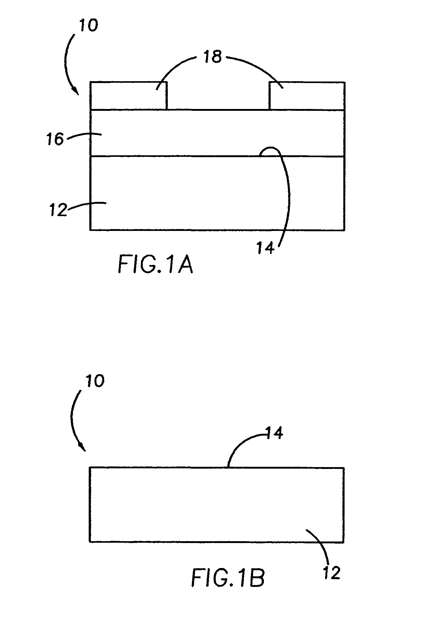
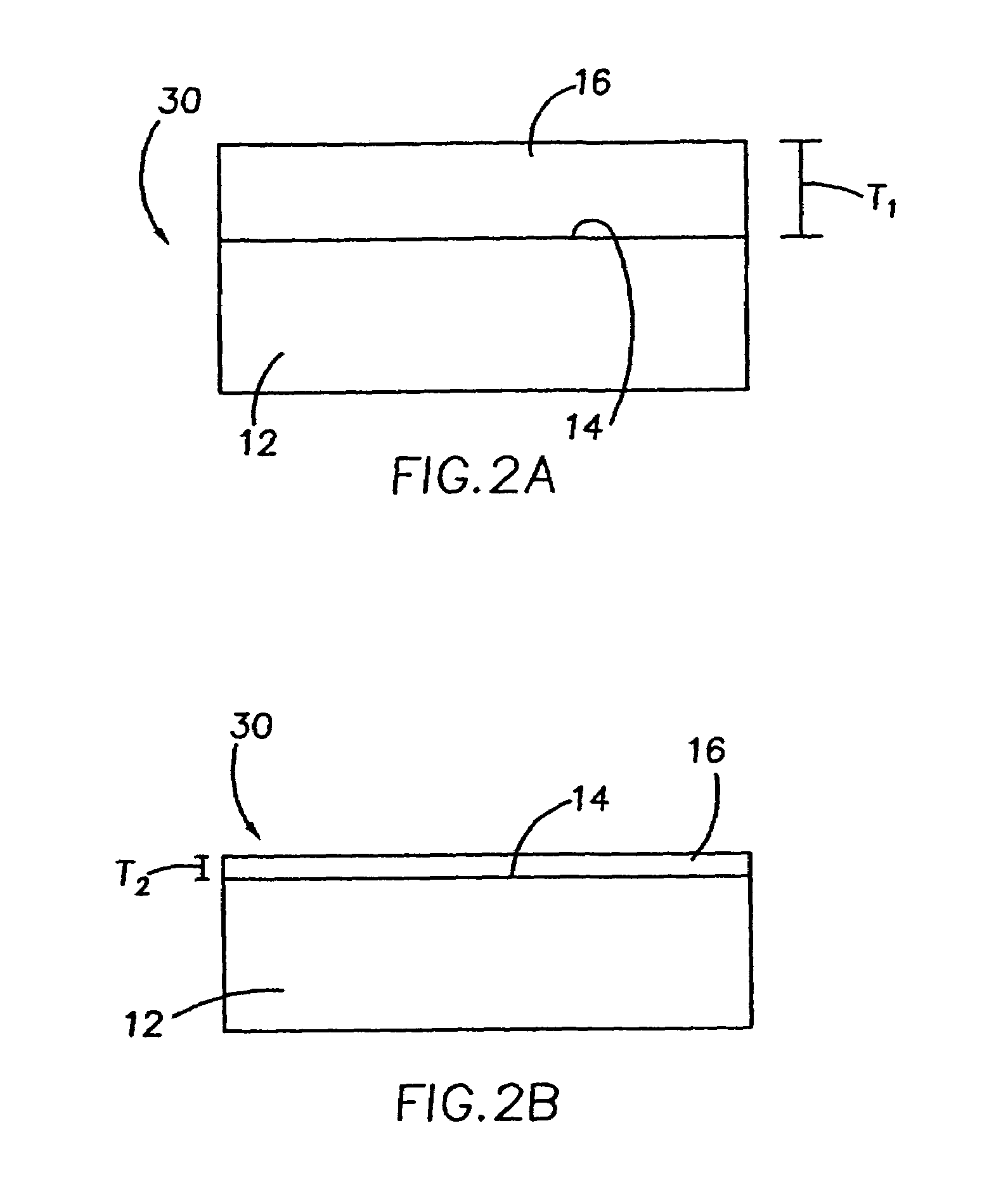
[0045]This example studies the effect of varying the fluorine-comprising component (49% HF or 40% NH4F), and the v / v ratios of the fluorine-comprising component and the acid component (50% citric acid) on the rate of removal of a low-k dielectric and a photoresist layer (OIR 897-10I) from a silicon wafer surface.

[0046]

TABLE 1Low-kremoval ratePhotoresistRun #Fluorine componentParts (v)Acid ComponentParts (v)(Å / min.)Removal149% HF100——anegligibleanegligible249% HF100——bnegligiblebnegligible340% NH4F250% citric acid1100negligible449% HF250% citric acid12500negligible549% HF150% citric acid2500complete649% HF150% citric acid100Negligiblecomplete7cHydrogen fluorine190% sulfuric acid5Complete (700)Completepyridinium (anhydride)aRepeated acid / water dips over 30 minutes, produced non-uniform flaking without dissolution of the low-k dielectric or photoresist.bA single, prolonged immersion (20+ minutes) showed little or no effect on removal of the low-k or 10i photoresist.cThe wafer surface h...


PUM

PropertyMeasurementUnit
percent by volumeaaaaaaaaaa

Abstract

An improved composition and method for cleaning the surface of a semiconductor wafer are provided. The composition can be used to selectively remove a low-k dielectric material such as silicon dioxide, a photoresist layer overlying a low-k dielectric layer, or both layers from the surface of a wafer. The composition is formulated according to the invention to provide a desired removal rate of the low-k dielectric and / or photoresist from the surface of the wafer. By varying the fluorine ion component, and the amounts of the fluorine ion component and acid, component, and controlling the pH, a composition can be formulated in order to achieve a desired low-k dielectric removal rate that ranges from slow and controlled at about 50 to about 1000 angstroms per minute, to a relatively rapid removal of low-k dielectric material at greater than about 1000 angstroms per minute. The composition can also be formulated to selectively remove a photoresist layer, leaving the underlying low-k dielectric layer essentially intact.

Description

CROSS-REFERENCE TO RELATED APPLICATIONS[0001]This application is a division of U.S. patent application Ser. No. 09 / 652,991, filed Aug. 31, 2000, now U.S. Pat. No. 6,762,132.FIELD OF THE INVENTION[0002]The present invention relates to compositions and methods for their use in cleaning or etching of wafers used in the fabrication of semiconductor devices. More particularly, the invention relates to compositions for selectively removing low-k dielectric layers and / or photoresist layers on the wafers while controlling the rate of removal of the material, and methods using the compositions.BACKGROUND OF THE INVENTION[0003]Many semiconductor processes require wafer measurements to be made from time to time for production-line quality control, product stability, and conformance to specifications. Generally, the processing results are evaluated after each significant step. Since many tests are destructive or will harm the product wafer, the measurements are typically performed on a test or ...

Claims


Application Information

Patent Timeline
Patent Type & Authority Patents(United States)
IPC IPC(8): H01L21/302B08B3/08C11D7/08C11D7/10C11D11/00G03F7/42H01L21/311
CPCB08B3/08C11D7/08C11D7/10C11D11/0047G03F7/423C11D7/50H01L21/31133C09K13/00C09K13/08H01L21/31111Y10S438/948C11D2111/22C23G1/02C09K13/04C09K13/06
Inventor YATES, DONALD L
Owner MICRON TECH INC
Features
  • Generate Ideas
  • Intellectual Property
  • Life Sciences
  • Materials
  • Tech Scout
  • Unparalleled Data Quality
  • Higher Quality Content
  • 60% Fewer Hallucinations
Learn More