Methods and array for creating a mathematical model of a plasma processing system

a plasma processing system and mathematical model technology, applied in plasma welding apparatus, plasma technique, manufacturing tools, etc., can solve the problems of increasing heat transfer rate, difficult to monitor plasma process, processing system cannot adequately compensate,

Inactive Publication Date: 2008-10-14
LAM RES CORP
View PDF4 Cites 43 Cited by
  • Summary
  • Abstract
  • Description
  • Claims
  • Application Information

AI Technical Summary

Benefits of technology

[0062]Advantages of the invention include methods and array for creating a mathematical model of a plasma processing system. Additional advantages include potentially precluding manufacturing defects caused by incorrectly installed, improperly manufactured or damaged components. Other advantages include calculating a simplified equivalent circuit model in a substantially automated fashion.

Problems solved by technology

That is, increasing helium pressure subsequently also increases the heat transfer rate.
However, with these and other plasma processes, it is often difficult to monitor the plasma process, and hence to preclude potential manufacturing defects caused by incorrectly installed, improperly manufactured, or damaged components.
However, since the electrostatic chuck (chuck) is no longer shielded by the substrate, it is subsequently etched.
Eventually, the plasma processing system cannot adequately compensate, and the process recipe's parameters are invalidated.
Since it is often impractical to determine when this point is exactly reached, the chuck is generally replaced after a certain amount of operational hours, which in practice is normally only a fraction of its useful life.
This can both increase productions costs, since an expensive chuck may be needless replaced, and reduces yield, since the plasma processing system must be taken offline for several hours to replace the chuck.
However, creating an empirical model may be problematic.
However, even a loosely correlated (and hence weakly predictive) model is difficult to obtain since repetition of the plasma process itself may effect of the electrical characteristics of plasma processing system components.
In addition, the extraction process may be difficult to automate, since the cost of a network analyzer may prohibit its integration into most plasma processing systems.

Method used


Image

  • Methods and array for creating a mathematical model of a plasma processing system
  • Methods and array for creating a mathematical model of a plasma processing system
  • Methods and array for creating a mathematical model of a plasma processing system

Examples


Embodiment Construction

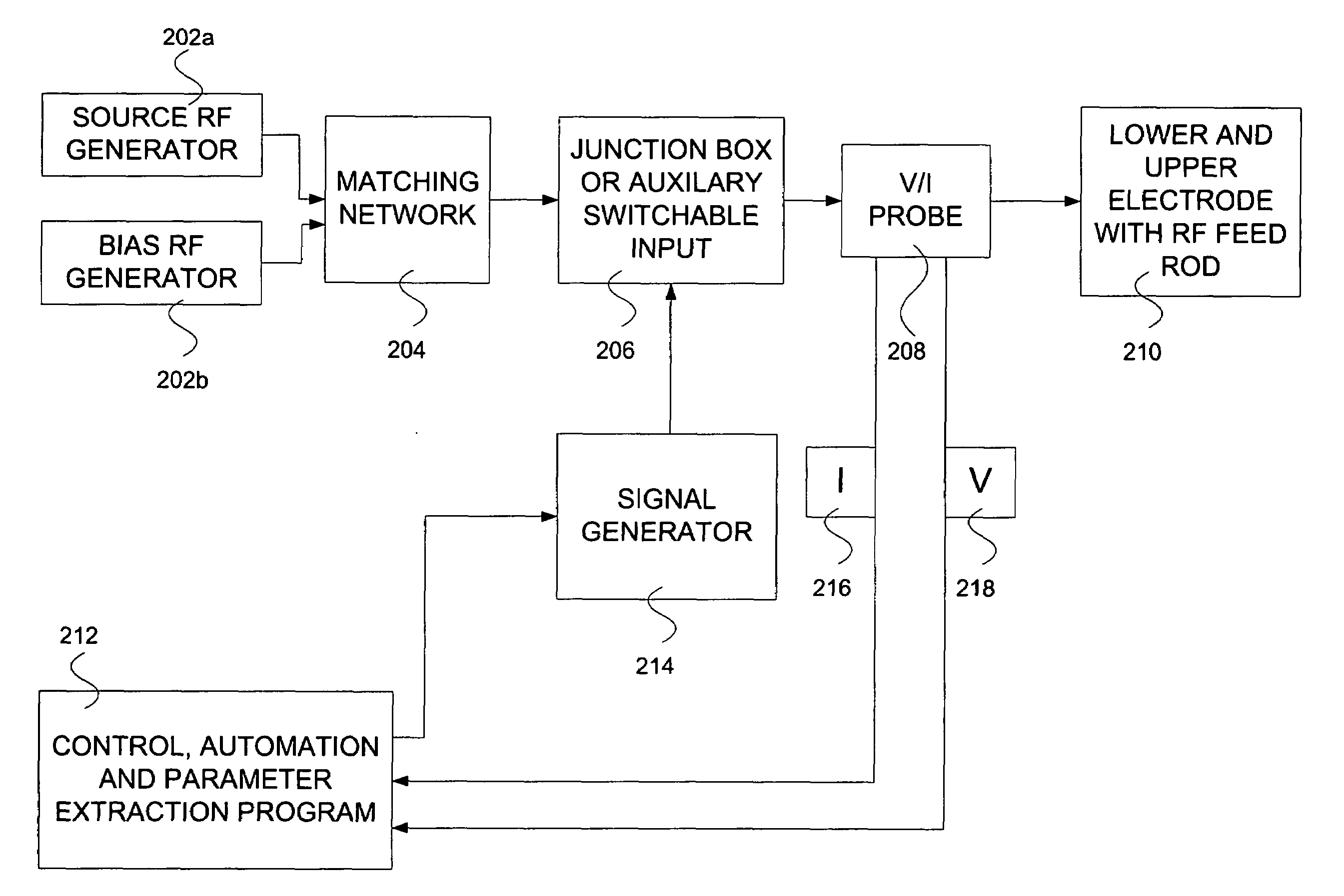
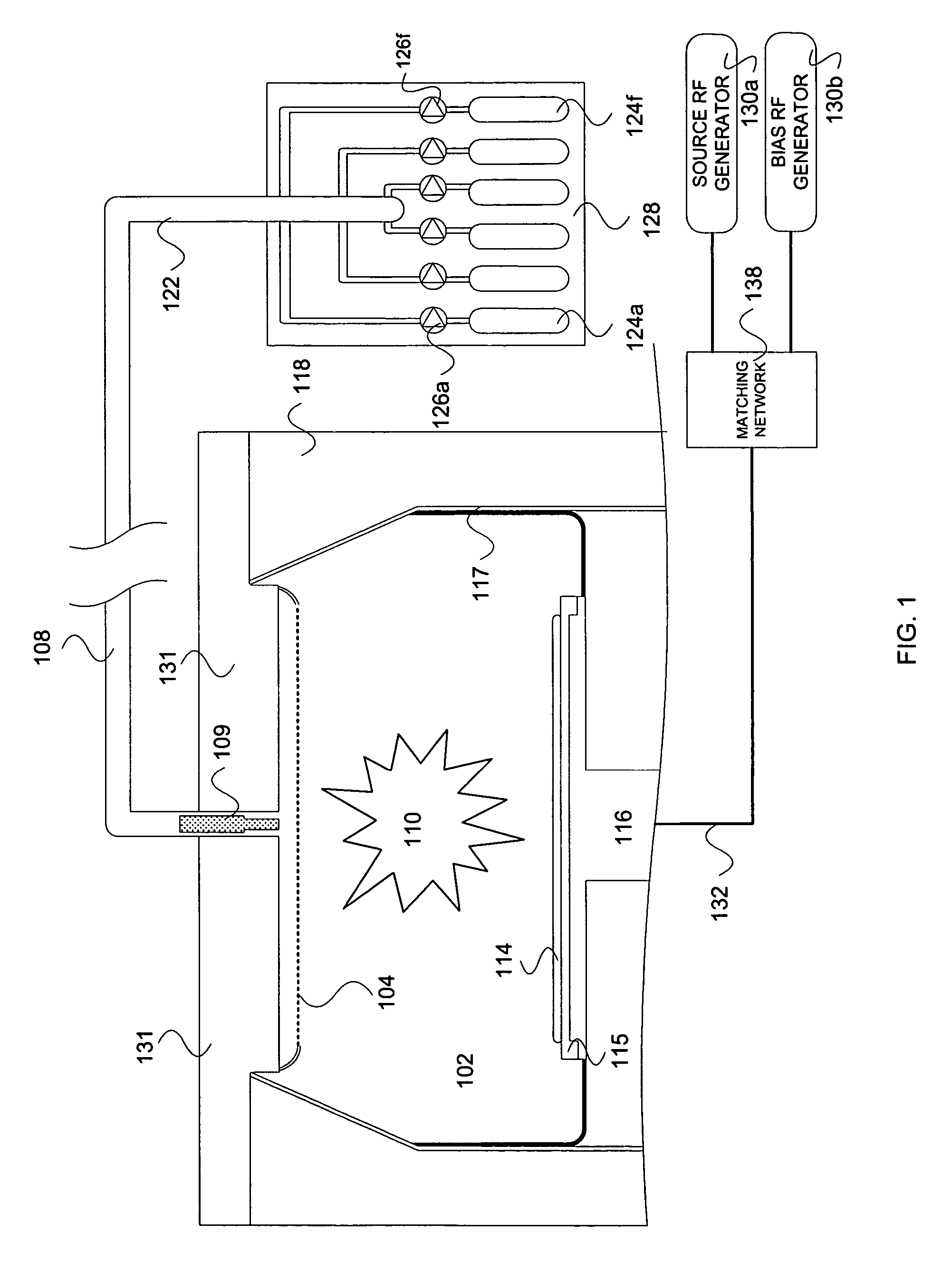
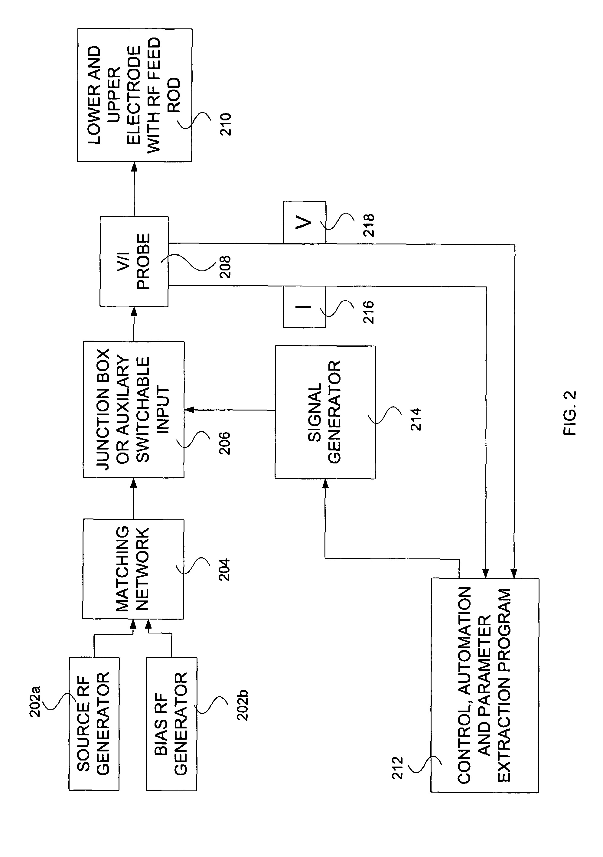
[0023]The present invention will now be described in detail with reference to a few preferred embodiments thereof as illustrated in the accompanying drawings. In the following description, numerous specific details are set forth in order to provide a thorough understanding of the present invention. It will be apparent, however, to one skilled in the art, that the present invention may be practiced without some or all of these specific details. In other instances, well known process steps and / or structures have not been described in detail in order to not unnecessarily obscure the present invention.

[0024]While not wishing to be bound by theory, it is believed by the inventor herein that a simplified model can be used to determine and / or predict potential problems in a plasma processing system. That is, a set of models can be created, and then subsequently compared, in order to determine potential manufacturing defects caused by incorrectly installed, improperly manufactured, or damag...


PUM

PropertyMeasurementUnit
parasitic capacitanceaaaaaaaaaa
frequenciesaaaaaaaaaa

Abstract

A method of creating a simplified equivalent circuit model of a plasma processing system, including an electrical measuring device, a lower electrode, an upper electrode, and a signal generator device is described. The method includes creating a simplified equivalent circuit equation, including a set of variables, of the plasma processing system, wherein the electrical measuring device comprises a first subset of variables, the lower electrode comprises a second subset of variables, the upper electrode comprises a third subset of variables, and the signal generator device comprises a forth subset of variables. The method also includes generating a set of signals, each of the set of signals being generated at a different frequency, wherein the signal generator device is coupled to the electrical measuring device, the lower electrode, and the upper electrode. The method further includes measuring the set of signals with the electrical measuring device, wherein at least one measured signal is generated for each of the set of variables; and, creating a simplified equivalent circuit model from the set of signals.

Description

BACKGROUND OF THE INVENTION[0001]The present invention relates in general to substrate manufacturing technologies and in particular to methods and array for creating a mathematical model of a plasma processing system.[0002]In the processing of a substrate, e.g., a semiconductor substrate or a glass panel such as one used in flat panel display manufacturing, plasma is often employed. As part of the processing of a substrate for example, the substrate is divided into a plurality of dies, or rectangular areas, each of which will become an integrated circuit. The substrate is then processed in a series of steps in which materials are selectively removed (etching) and deposited (deposition) in order to form electrical components thereon.[0003]In an exemplary plasma process, a substrate is coated with a thin film of hardened emulsion (i.e., such as a photoresist mask) prior to etching. Areas of the hardened emulsion are then selectively removed, causing components of the underlying layer ...

Claims


Application Information

Patent Timeline
Patent Type & Authority Patents(United States)
IPC IPC(8): B23K10/00C23F1/00H01J37/00H01J37/32H01L21/00H01L21/205H01L21/3065H05H1/00H05H1/46
CPCH01J37/32082H01J37/32935H05H1/46
Inventor JAFARIAN-TEHRANI, SEYED JAFAR
Owner LAM RES CORP
Why Eureka
Try Eureka