Current-output type digital-to-analog converter

a converter and digital-to-analog technology, applied in the field of current-output type digital-to-analog converters, can solve the problems of reducing conversion accuracy, difficult to keep good linearity of the operational amplifier and requiring good linearity in the wide range of input voltage. achieve the effect of higher accuracy

Inactive Publication Date: 2008-10-28
ROHM CO LTD
View PDF6 Cites 11 Cited by
  • Summary
  • Abstract
  • Description
  • Claims
  • Application Information

AI Technical Summary

Benefits of technology

[0010]In view of the foregoing, a general purpose of the invention is to provide a current-output type digital-to-analog converter having higher accuracy.
[0014]The current flowing through each output transistor can be stabilized by fixing the voltage at one end of the input transistor to the reference voltage, and the accuracy of the digital-to-analog converter can be improved.
[0018]In this case, because the voltage at the current output terminal is equal to the voltage at the second terminal of the input transistor, the same potentials are obtained at the three terminals in the input transistor and the n output transistors. Therefore, the current can accurately be generated according to the size ratio of the transistors, and the accuracy of the digital-to-analog conversion can be improved.
[0021]In this case, because the input transistor and the n output transistors are operated in the non-constant current region, the voltage drop across each transistor can be reduced, and the power consumption can be decreased. The conventional current-mirror circuit is operated in the non-constant current region, which affects the mirror ratio. On the other hand, according to the embodiment of the invention, because the same potentials are obtained at the three terminals in the input transistor and the output transistor, the current can flow through each transistor according to the area ratio, and the digital-to-analog conversion is realized with high accuracy.
[0024]According to the embodiment of the invention, the current flowing through the load can accurately be switched according to the digital value.
[0026]According to the embodiment of the invention, brightness of the light emitting device can accurately be adjusted with the reference current.

Problems solved by technology

Therefore, there is a problem that good linearity is required in the wide range of input voltage for in voltage-to-current conversion circuit.
In many cases, the voltage-to-current conversion circuit is designed using an operational amplifier, and it is very difficult to keep good linearity of the operational amplifier in the wide range of input voltage.
Accordingly, in the current-output type digital-to-analog converter of the above-mentioned type, there is a problem that conversion accuracy is decreased.

Method used


Image

  • Current-output type digital-to-analog converter
  • Current-output type digital-to-analog converter
  • Current-output type digital-to-analog converter

Examples


first embodiment

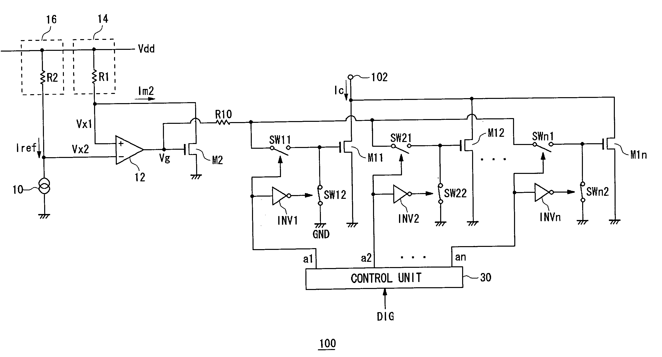
[0037]FIG. 1 is a circuit diagram showing a configuration of a current-output type digital-to-analog converter 100 (hereinafter also referred to as current DAC 100) according to a first embodiment of the invention.

[0038]The current DAC 100 receives n-bit (n is a natural number) digital signal DIG, and the current DAC 100 outputs a constant electric current Ic according to the input digital signal DIG from a current output terminal 102.

[0039]The current DAC 100 includes n (n is a natural number) output transistors M11 to M1n, an input transistor M2, a constant current source 10, a first error amplifier 12, a first current-to-voltage conversion unit 14, and a second current-to-voltage conversion unit 16.

[0040]The output transistors M11 to M1n are N-type MOSFETs, each of which having a first terminal, that is a source, is fixed by a common fixed voltage, that is a ground voltage, and a second terminal located on a side opposite the first terminal, that is a drain, is connected to a cur...

second embodiment

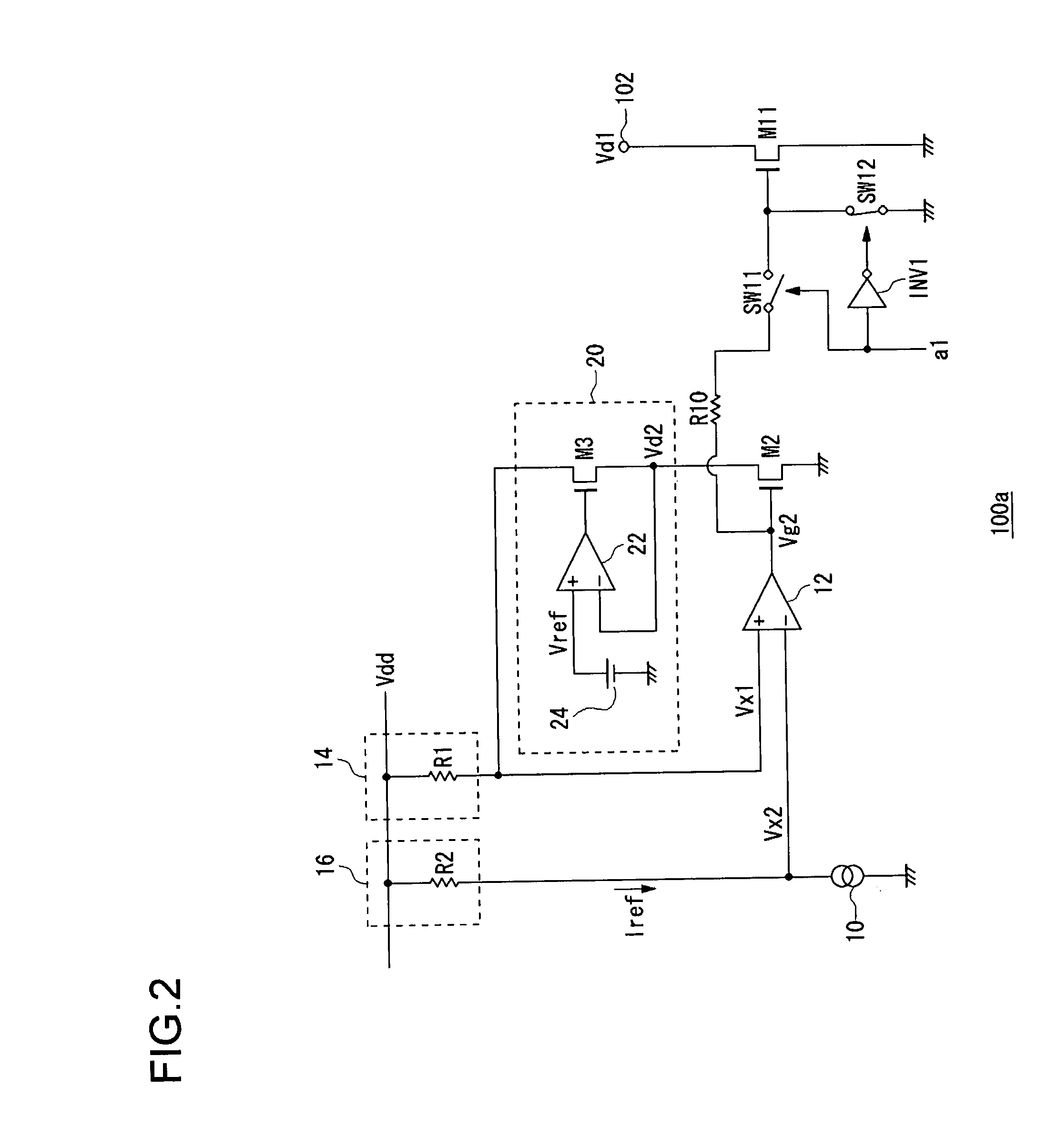
[0056]A current DAC 100a according to a second embodiment further includes a voltage adjustment unit 20 which fixes the drain voltage of the input transistor M2 in addition to the current DAC 100 of the first embodiment.

[0057]FIG. 2 is a circuit diagram showing a configuration of a current DAC 100a according to a second embodiment. In the following drawings, the same or equivalent component as the first embodiment is denoted by the same numeral, descriptions will not be repeated.

[0058]The voltage adjustment unit 20 is connected between the first resistor R1 and the drain which is of one end of the input transistor M2, and the voltage adjustment unit 20 makes an adjustment such that a voltage Vd2 at the drain of the input transistor M2 is brought close to a predetermined reference voltage. In FIG. 2, the output transistors M12 to M1n are not shown. The voltage adjustment unit 20 includes an adjustment transistor M3, a second error amplifier 22, and a reference voltage source 24, to c...

third embodiment

[0073]A current DAC 100b according to a third embodiment is a modification of the current DAC 100a of the second embodiment and the configuration of the current-to-voltage conversion unit 14 differs from that in the second embodiment. FIG. 4 is a circuit diagram showing a configuration of a current DAC 100b according to this embodiment. In FIG. 4, the output transistors M12 to M1n are not shown as in FIG. 2.

[0074]A first current-to-voltage conversion unit 14b of FIG. 4 includes a first detection transistor M4, a second detection transistor M5, and a first reference resistor R11. The first detection transistor M4 is provided on the same current path as the input transistor M2. The first detection transistor M4 is a P-type MOSFET in which the source is connected to the power supply terminal and the drain and gate are connected to the drain of the adjustment transistor M3. The second detection transistor M5 is connected to the first detection transistor M4 in the current-mirror manner....


PUM


Abstract

Source potentials of n output transistors are fixed by common fixed voltage, and sources are connected to a current output terminal. A drain and a gate of an input transistor are commonly connected to the drains and the gates of the output transistors respectively. A first current-to-voltage conversion unit is connected onto the drain side of the input transistor to convert current Im2 flowing through the input transistor into voltage Vx1. A second current-to-voltage conversion unit converts reference current Iref into voltage Vx2. The voltages Vx1 and Vx2 are input to a first error amplifier, and the first error amplifier adjusts gate voltages of the input transistor and output transistors. n switches are provided on a path through which output of the first error amplifier reaches the gate of the output transistor. A control unit controls on / off of the switch according to a digital signal.

Description

BACKGROUND OF THE INVENTION[0001]1. Field of the Invention[0002]The present invention relates to a current-output type digital-to-analog converter which generates and outputs an output electric current according to an input digital signal.[0003]2. Description of the Related Art[0004]Recently, in a field of compact information terminals such as a portable telephone and PDA (Personal Digital Assistance), there is a device requiring higher voltage than an output voltage of a battery, such as a light emitting diode (hereinafter referred to as LED) used in a back light of a liquid crystal display. In such compact information terminals, a lithium ion battery is frequently used. The output voltage of lithium ion battery is usually about 3.5V, and about 4.2V even in a fully-charged state. However, the voltage higher than the battery voltage is required as the drive voltage of an LED. In the case where the voltage higher than the battery voltage is required, the battery voltage is boosted to...

Claims


Application Information

Patent Timeline
Patent Type & Authority Patents(United States)
IPC IPC(8): H03M1/66
CPCH03M1/0612H03M1/745
Inventor CHIDA, TAISUKEKOMIYA, KUNIHIRO
Owner ROHM CO LTD
Why Eureka
Try Eureka