Semiconductor laser element and semiconductor laser element array

a laser element and semiconductor technology, applied in the direction of lasers, semiconductor lasers, optical resonator shape and construction, etc., can solve the problems of complex lens shape, high manufacturing cost, and small area of the emitting end, so as to reduce the emission angle reduce the effect of manufacturing cos

Inactive Publication Date: 2008-11-04
HAMAMATSU PHOTONICS KK
View PDF10 Cites 6 Cited by
  • Summary
  • Abstract
  • Description
  • Claims
  • Application Information

AI Technical Summary

Benefits of technology

[0024]In accordance with the present invention, a semiconductor laser element and semiconductor laser element array, which can efficiently emit relatively high intensity laser beams with a small emission angle, and having a single peak horizontal emission pattern, can be provided using a simpler configuration.

Problems solved by technology

However, when the width of the waveguide is narrow, the area of the emitting end also becomes small.
The multi-mode type semiconductor laser element, however, has the following problem.
So the shape of the lens to condense or collimate the laser beams becomes complicated, and desired laser beams may not be acquired or the manufacturing cost may become high (lens becomes expensive).

Method used


Image

  • Semiconductor laser element and semiconductor laser element array
  • Semiconductor laser element and semiconductor laser element array
  • Semiconductor laser element and semiconductor laser element array

Examples


first embodiment

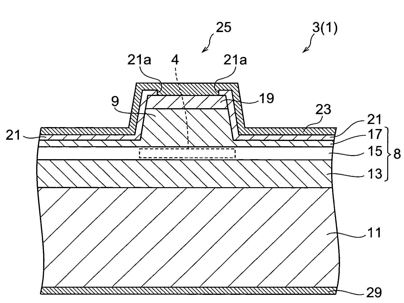
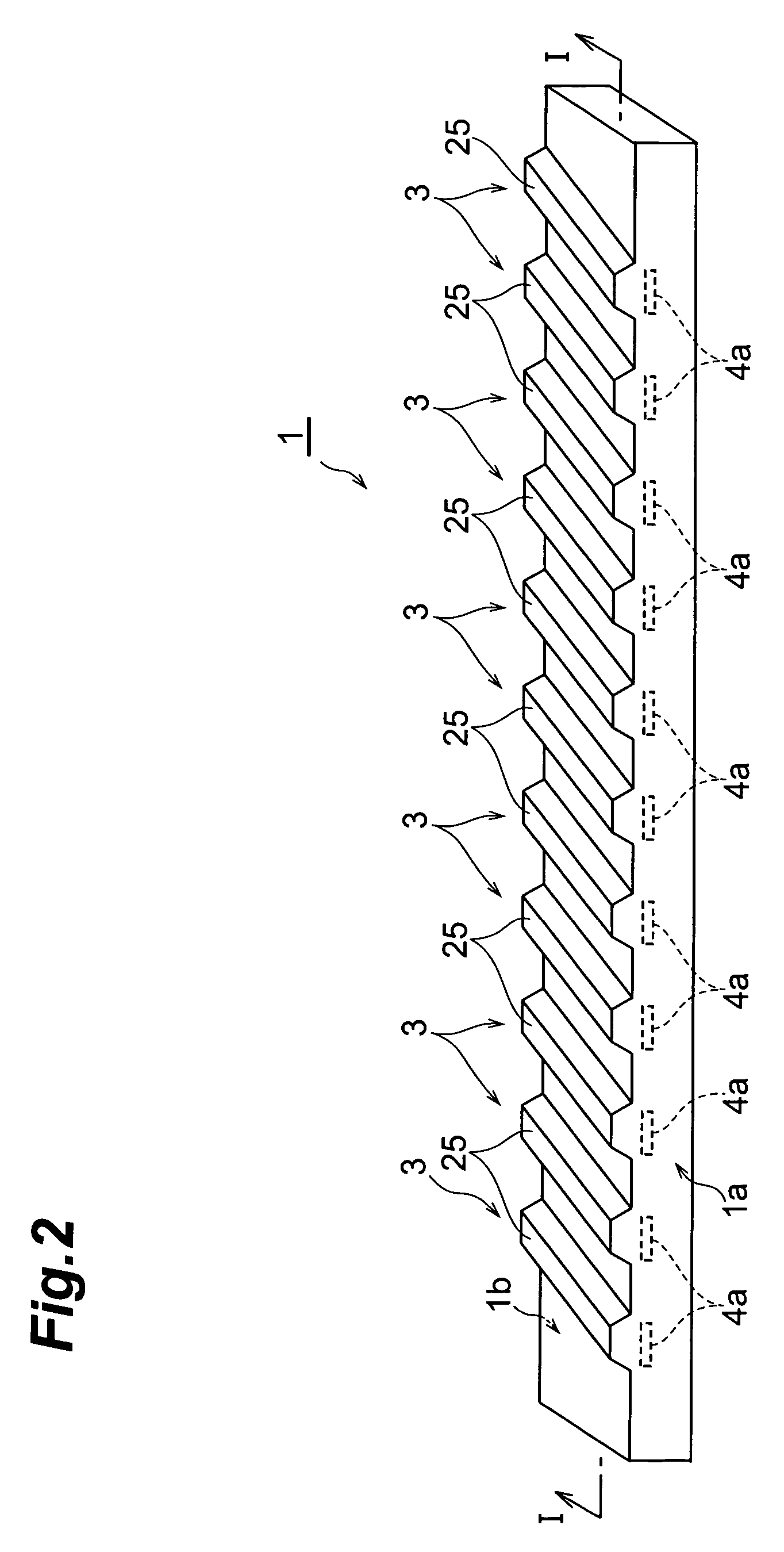
[0050]FIG. 2 is a perspective view showing the configuration of the semiconductor laser element array to which the first embodiment of the semiconductor laser element according to the present invention is applied (an embodiment of the semiconductor laser element array according to the present invention). As shown in FIG. 2, the semiconductor laser element array 1 has a plurality of semiconductor laser elements 3 which have an integral structure. The number of semiconductor laser elements 3 of the semiconductor laser element array 1 can be arbitrary, and when there is only one, it is not an array but a single semiconductor laser element. The semiconductor laser element array 1 has a light emitting face 1a and light reflecting face 1b, which face each other, and on the light emitting face 1a, a laser beam emitting end 4a of each semiconductor laser element 3 is placed in the horizontal direction. Each of the plurality of semiconductor laser elements 3 has a convex portion 25 which is ...

first application example of first embodiment

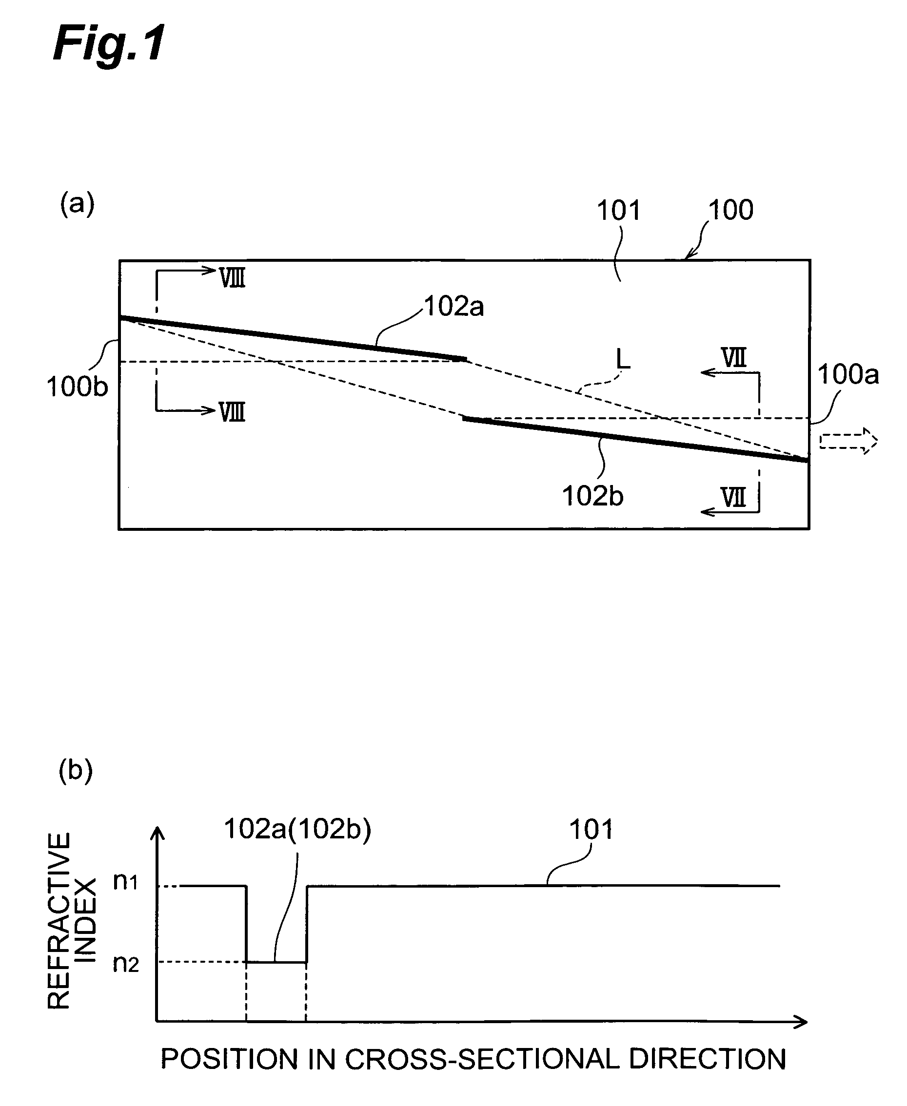
[0076]Next, a first application example of the semiconductor laser element 3 according to the first embodiment will be explained. In the first application example, the angle θ formed by the side faces 4c and 4d of the refractive index type waveguide 4 and the direction A, which matches each normal line of the light emitting end 4a and the light reflecting end 4b, is set to the critical complementary angle 4° based on the refractive index difference between the inside and outside the refractive index type waveguide 4. The space between the side face 4c and side face 4d of the refractive index type waveguide 4 (width of the refractive index type waveguide 4) is 40 μm, and the distance between the laser beam emitting end 4a and the laser beam reflecting end 4b (length of the refractive index type waveguide 4) is set to 1200 μm, which can implement the optical path in FIG. 7. The waveguide width of a conventional single mode type semiconductor laser element (including the semiconductor ...

second application example of first embodiment

[0080]Next, as a second application example of the first embodiment, a semiconductor element array 1, having a plurality of semiconductor laser elements each of which have the same structure of the semiconductor laser element 3 of the first embodiment having the above structure, will be explained. In the second application example, 50 ridge portions are formed in 1 cm with a 200 μm pitch. The area (a) of FIG. 12 is a graph showing the current vs. optical output characteristics of the semiconductor laser element array of the second application example. As shown in the graph of the area (a), the current supplied to each semiconductor laser element of the semiconductor laser element array and the laser beam output has a linear correlation, and kinks are not generated. The slope efficiency of the element according to this graph is 0.75 W / A, which is equivalent to the case of a single semiconductor laser element (see FIG. 10). Therefore, as compared with the resonator of the Internationa...


PUM


Abstract

The present invention relates to a semiconductor laser element and the like which can efficiently emit laser beams at a small emission angle using a simpler configuration. The semiconductor laser element has a structure where an n-type cladding layer, active layer and p-type cladding layer are sequentially laminated. The p-type cladding layer has a ridge portion for forming a refractive index type waveguide in the active layer. The ridge portion, at least the portion excluding the edges, extends in a direction crossing each normal line of both end faces of the refractive index type waveguide, which corresponds to the light emitting face and light reflecting face respectively, at an angle θ, which is equal to or less than the complementary angle θc of the total reflection critical angle on the side face of the refractive index type waveguide. The optical paths of light components which resonate in the refractive index type waveguide formed by the ridge portion having the above form are limited to optical paths where the lights are totally reflected on the side face of the refractive index type waveguide. In other words, the laser beams emitted from the light emitting end have a spatial horizontal single mode, and the waveguide width can be increased to further decrease the emission angle of the laser beams.

Description

TECHNICAL FIELD[0001]The present invention relates to a semiconductor laser element, and a semiconductor laser element array which includes the semiconductor laser elements.BACKGROUND ART[0002]As a semiconductor laser element, a spatial horizontal single mode type one and a multi-mode type one are always known. In a single mode type semiconductor laser element, a waveguide with a narrow width is formed to limit the oscillation mode in the waveguide to only a single mode. However, when the width of the waveguide is narrow, the area of the emitting end also becomes small. When the laser beam density becomes excessively high at the emitting end, reliability of the semiconductor laser element is influenced. Therefore, the single mode type semiconductor laser element is suitable for applications where relatively low output laser beams are used. An example of the single mode type semiconductor laser element is the semiconductor laser device disclosed in Patent Document 1. This semiconduct...

Claims


Application Information

Patent Timeline
Patent Type & Authority Patents(United States)
IPC IPC(8): H01S5/00H01S3/08H01S5/22
CPCH01S5/10H01S5/22H01S5/4031H01S5/0655H01S5/101H01S5/1085H01S5/2036H01S2301/18
Inventor MIYAJIMA, HIROFUMIWATANABE, AKIYOSHIKAN, HIROFUMI
Owner HAMAMATSU PHOTONICS KK
Why Eureka
Try Eureka