Vertical electrode structure of gallium nitride based light emitting diode

a technology of light-emitting diodes and vertical electrodes, which is applied in the manufacture of semiconductor/solid-state devices, electrical equipment, and semiconductor devices. it can solve the problems of short life, high manufacturing cost, and failure of present used traffic signals of lamps, so as to reduce the loss of fresnel refraction, facilitate reflection, and advance the effect of external luminous efficiency

Active Publication Date: 2008-11-18
LUMENS
View PDF1 Cites 22 Cited by
  • Summary
  • Abstract
  • Description
  • Claims
  • Application Information

AI Technical Summary

Benefits of technology

[0008]The main purpose of the present invention is to offer a vertical electrode structure of a kind of GaN-based light emitting diode—the GaN-based light emitting diode, which utilizes an oxide window layer, constitutes a good ohmic contact with a N-type ohmic contact layer, conductivity and transparency. Additionally, as to the specific refraction index locates between 1.85-2.0, it can facilitate to reduce the Fresnel refraction loss and total reflection so as to advance the external luminous efficiency.
[0009]The second purpose of this invention is to offer a vertical electrode structure of a kind of GaN-based light emitting diode, wherein a metal reflection layer is used to facilitate the reflection without selective angle of incidence so as to enlarge the angle of incidence. Therefore, it is capable of effectively reflecting the light emitted from the light emitting layer and advances the function of heat eliminating and electrostatic discharge (ESD) due to vertical electrode structure. Further, its operating life can be prompted and it is applicable to the using in high current driving.
[0010]Another purpose of the present invention is to offer a vertical electrode structure of a kind of GaN-based light emitting diode, wherein the disclosed vertical electrode structure can decrease the manufacturing area of chip and facilitate the conventional wire bonding process.
[0011]To achieve the afore-mentioned purposes and advantages, the present invention is related to a vertical electrode of a kind of GaN-based light emitting diode including: a first electrode, a conductive substrate on said first electrode, a metal reflection layer with said conductive substrate there-under, a GaN-based semiconductor stacked structure with said metal reflection layer there-under, an oxide window layer on said GaN-based semiconductor stacked structure, and a second electrode with said oxide window layer there-under. The oxide window layer constructs the vertical electrode of GaN-based light emitting diode, and effectively reduce Fresnel refraction loss and total reflection, and further advances the external luminous efficiency. In addition, the further included metal reflection layer advances the reflection without selective angle of incidence, thus increasing the bandwidth of reflecting angles and effectively reflecting the light emitted from the light emitting layer. Moreover, such kind of structure can prompt the function of heat eliminating and the electrostatic discharge, so its operating life can be raised and it is applicable to the using of high current driving. Finally, the vertical electrode structure of the present invention can decrease the manufacturing area of chip and facilitate the conventional wire bonding process.

Problems solved by technology

In addition, the present used traffic signals of lamp have the failures of energy consuming, short life, and the phantom image of illuminating (which occurs as the sunlight reflects off the display surface and easily causes the traffic accident).
Although the silicon carbide substrate with the conductive characteristic can be made into vertical electrode, the manufacturing cost is very expensive.
However, it has to make the lateral electrode structure if adopting the insulating substrate, which contributes the unavailability of the vertical electrode.
This being the case, it would take the special wire bonding apparatus and packing technology, and additionally, the manufacturing area of chip will also increase relatively, thus complicating the manufacturing process and increase the cost of each component.

Method used


Image

  • Vertical electrode structure of gallium nitride based light emitting diode
  • Vertical electrode structure of gallium nitride based light emitting diode
  • Vertical electrode structure of gallium nitride based light emitting diode

Examples


example 1

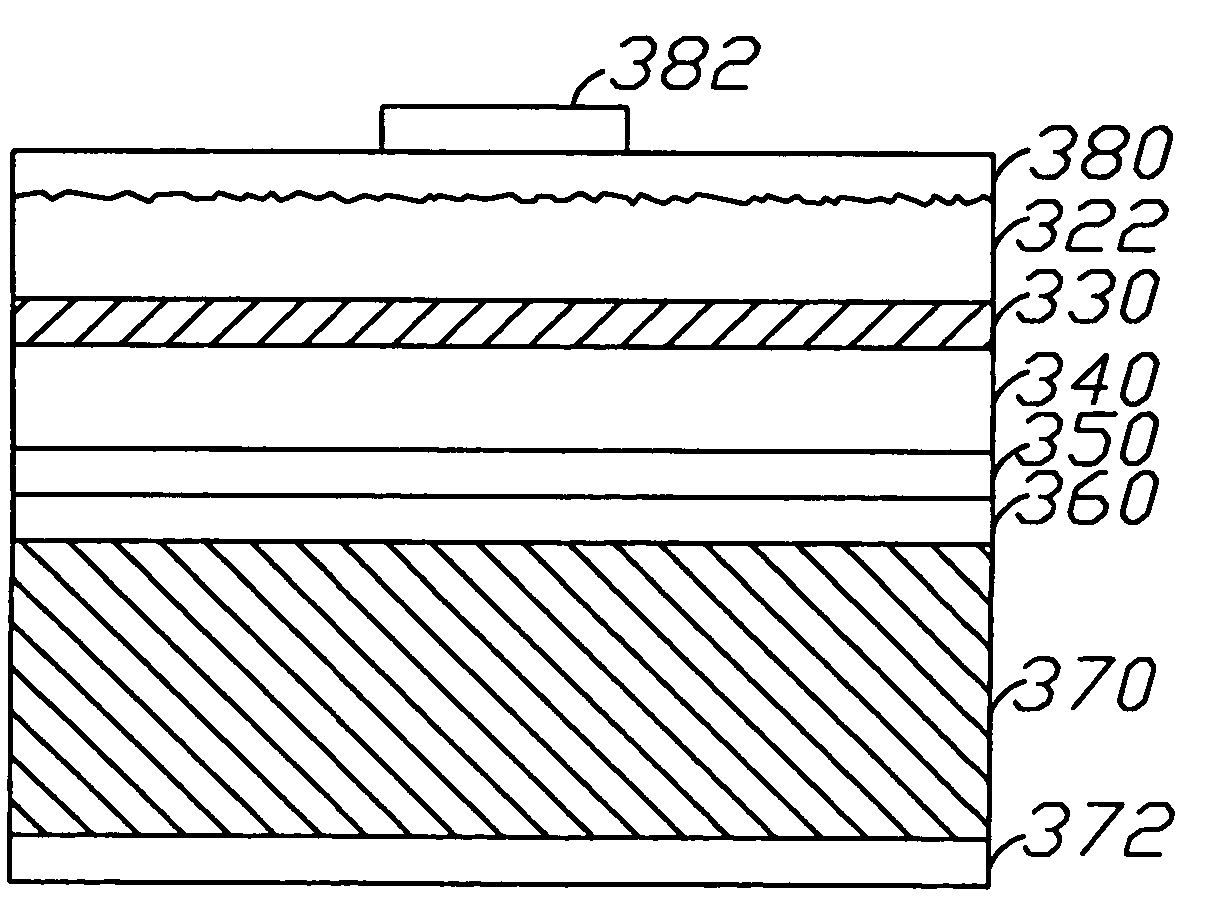
[0013]As shown in FIG. 3A, which is one of the embodiment of this invention, first of all, on a sapphire substrate 300, sequentially epitaxize a low temperature GaN buffer layer 310, a N-type AlInGaN ohmic contact layer 320, a AlInGaN light emitting layer 330, and a P-type AlInGaN ohmic contact layer 340. Following, a transparent ohmic contact metal layer 350 and a metal reflection layer 360 are subsequently formed on the P-type AlInGaN ohmic contact layer 340 by evaporating or sputtering technologies as shown in FIG. 3B. Then, the other conductive substrate 370 is bonded with the metal reflection layer 360 by thermal bonding as shown in FIG. 3C. Then, the FIG. 3D depicts that the sapphire substrate 10 is removed by laser liftoff or lapping technologies. And as shown in FIG. 3E, after laser liftoff, the remaining gallium metal on the surface of N-type AlInGaN ohmic contact layer 12 is removed by chemical etching to expose the N-type AlInGaN ohmic contact layer 320, and then, the N-t...

example 2

[0014]As shown in FIG. 3A, which is another embodiment of this invention, first of all, on the sapphire substrate 300, sequentially epitaxize a low temperature GaN buffer layer 310, a N-type AlInGaN ohmic contact layer 320, a AlInGaN light emitting layer 330, and a P-type AlInGaN ohmic contact layer 340. Then a transparent ohmic contact metal layer 350 and a metal reflection layer 360 are subsequently formed on the P-type AlInGaN ohmic contact layer by evaporating or sputtering technologies as shown in FIG. 3B. As the depiction in FIG. 3C, another conductive substrate 370 is bonded with said metal reflection layer 360 by thermal bonding. Following, the sapphire substrate is removed by laser liftoff or lapping as shown in FIG. 3D. After laser liftoff, then, the remaining gallium metal on the surface of N-type AlInGaN ohmic contact layer 320 is eliminated by chemical etching to expose the N-type AlInGaN ohmic contact layer 320. Subsequently, the N-type transparent metal oxide layer 38...

example 3

[0015]As shown in FIG. 3A, which is another embodiment of the present invention, first of all, on the sapphire substrate 300, sequentially, epitaxize a low temperature GaN buffer layer 310, a N-type AlInGaN ohmic contact layer 320, a AlInGaN light emitting layer 330, and a P-type AlInGaN ohmic contact layer 340. Then a transparent ohmic contact metal layer 350 and a metal reflection layer 360 are subsequently formed on the P-type AlInGaN ohmic contact layer 340, as shown in FIG. 3B. Following, another conductive substrate 370 is bonded with said metal reflection layer 360 by thermal bonding as shown in FIG. 3C. Subsequently, the sapphire substrate 300 is removed by laser liftoff as the depiction in FIG. 3D. Then, the remaining gallium metal on the surface of the N-type AlInGaN ohmic contact layer 320 is eliminated by chemical etching to expose the N-type AlInGaN ohmic contact layer 320. And then the surface of N-type AlInGaN ohmic contact layer 320 is textured into a textured N-type...


PUM


Abstract

A vertical electrode structure of GaN-based light emitting diode discloses an oxide window layer constructing the GaN-based light emitting diode of vertical electrode structure, which effectively decreases the Fresnel reflection loss and total reflection, and further advances the luminous efficiency. Moreover, the further included metal reflecting layer causes the reflection without the selective angle of incidence, thus increasing the coverage of the reflecting angles and further reflecting the light emitted from a light emitting layer effectively. In addition, the invented structure can also advance the function of heat elimination and the electrostatic discharge (ESD) so as to the increase the operating life of the component and to be applicable to the using under the high current driving. Moreover, the vertical electrode structure of the present invention is able to lower down the manufacturing square of the chip and facilitate the post stage of the conventional wire bonding process.

Description

[0001]This application is a Divisional patent application of co-pending application Ser. No. 10 / 986,126, filed on 12 Nov. 2004.BACKGROUND OF THE INVENTION [0002]1. Field of the Invention[0003]The present invention is related to a kind of vertical electrode structure of GaN-based light emitting diode. The GaN-based light emitting diode especially refers to a kind of diode with vertical electrode structure, which can effectively reduce Fresnel refraction loss and the total reflection, and further advance the external luminous efficiency.[0004]2. Description of the Related Art[0005]Accordingly, the application purpose to study the blue light emitting diode is to manufacture the full-color display, traffic light, and luminescent source. Nowadays, the prevailing various light emitting diodes in the market so far are with a variety of lights including red, green, orange, and yellow lights. However, as to the blue and green light emitting diodes, the practical degrees of high efficiency an...

Claims


Application Information

Patent Timeline
Patent Type & Authority Patents(United States)
IPC IPC(8): H01L33/00H01L29/22H01L33/14H01L33/22H01L33/32H01L33/38H01L33/40H01L33/42
CPCH01L33/0079H01L33/145H01L33/32H01L33/405H01L33/22H01L33/387H01L33/42H01L33/0093
Inventor LAI, MU-JENHON, SCHANG-JING
Owner LUMENS
Why Eureka
Try Eureka