Method of manufacturing color filter substrate, method of manufacturing electro-optical device, electro-optical device, and electronic apparatus

a technology of color filter substrate and electro-optical device, which is applied in the direction of lighting and heating apparatus, liquid/solution decomposition chemical coating, and domestic cooling apparatus, etc. it can solve the problems of insufficient dissolved irregularity in the film thickness of the functional layer of the electro-optical device, display irregularity may occur, and color irregularity may be small, and the effect of small irregularity in the element characteristi

Inactive Publication Date: 2008-12-02
KATEEVA
View PDF25 Cites 34 Cited by
  • Summary
  • Abstract
  • Description
  • Claims
  • Application Information

AI Technical Summary

Benefits of technology

[0008]An advantage of the invention is that it provides a method of manufacturing a color filter substrate which is capable of forming coloring patterns having a uniform film thickness on the surface thereof and a method of manufacturing an electro-optical device which is capable of forming pixel patterns having a uniform film thickness. Further, another advantage of the invention is that it provides an electro-optical device which is manufactured by such a manufacturing method and an electronic apparatus having the electro-optical device.
[0009]According to a first aspect of the invention, there is provided a method of manufacturing a color filter substrate which has a functional region including a plurality of colored layers and functioning as a color filter to selectively transmit predetermined color light components and a non-functional region other than the functional region. The method of manufacturing a color filter substrate includes discharging, onto a substrate, a liquid material, in which coloring materials constituting the colored layers are dissolved or dispersed into a solvent, with a liquid droplet discharge method. In the discharging of the liquid material, the liquid material is discharged onto the functional region and the liquid material or the solvent is discharged onto the non-functional region. The amount of the solvent discharged onto the non-functional region per unit area is larger than the amount of the solvent discharged onto the functional region per unit area.
[0010]In accordance with the first aspect of the invention, the amount of the solvent discharged onto the non-functional region per unit area is larger than the amount of the solvent discharged onto the functional region per unit area. Thus, when the solvent is dried after being discharged, the partial pressure of solvent particles to be evaporated in the functional region is not extremely larger than the partial pressure of the solvent particles to be evaporated in the non-functional region. For this reason, the evaporation speed of the solvent in the non-functional region can approximate to the evaporation speed of the solvent in the functional region. Therefore, the evaporation speed of the solvent in the peripheral portion of the functional region can approximate to the evaporation speed of the solvent in the central portion. As a result, the colored layers having the same thickness can be formed further uniformly in the peripheral portion and the central portion. Then, in this case, it is possible to provide a color filter substrate having small color irregularity and excellent reliability in the entire functional region, in particular, irregardless of the central portion or the peripheral portion.
[0011]According to a second aspect of the invention, there is provided a method of manufacturing an electro-optical device which has a functional region in which electro-optical elements of pixels function and a non-functional region which is formed around the functional region. The method of manufacturing an electro-optical device includes discharging, onto a substrate, a liquid material, in which functional materials constituting the electro-optical elements are dissolved or dispersed into a solvent, with a liquid droplet discharge method. In the discharging of the liquid material, the liquid material is discharged onto the functional region and the liquid material or the solvent is discharged onto the non-functional region. The amount of the solvent discharged onto the non-functional region per unit area is larger than the amount of the solvent discharged onto the functional region per unit area.
[0012]In accordance with the second aspect of the invention, the amount of the solvent discharged onto the non-functional region per unit area is larger than the amount of the solvent discharged onto the functional region per unit area. Thus, when the solvent is dried after being discharged, the partial pressure of solvent particles to be evaporated in the functional region is not extremely larger than the partial pressure of the solvent particles to be evaporated in the non-functional region. For this reason, the evaporation speed of the solvent in the non-functional region can approximate to the evaporation speed of the solvent in the functional region. Therefore, the evaporation speed of the solvent in the peripheral portion of the functional region can approximate to the evaporation speed of the solvent in the central portion. As a result, layers constituting an electro-optical element (electro-optical device element layers) having the same thickness can be formed further uniformly in the peripheral portion and the central portion. Then, in this case, it is possible to provide an electro-optical device having small irregularity in element characteristic and excellent reliability in the entire functional region, in particular, irregardless of the central portion or the peripheral portion.
[0013]The method of manufacturing an electro-optical device may further include, before the discharging of the liquid material, forming liquid holding regions in which the liquid material and / or the solvent are discharged in the same pattern (that is, in the respective regions, the patterns having the same shape and the same area are formed at regular intervals) onto the functional region and the non-functional region on the substrate, respectively. In this case, in the discharging of the liquid material, the amount of the solvent discharged onto the liquid holding region of the non-functional region may be larger than the amount of the solvent discharged onto the liquid holding region of the functional region. In such a manner, the amount of the solvent discharged onto the non-functional region per unit area can be larger than the amount of the solvent discharged onto the functional region per unit area. As a result, the advantages of the invention can be properly realized.

Problems solved by technology

As a result, irregularity in film thickness of the functional layer may occur in the electro-optical device.
Further, when the electro-optical device is used in a display device or the like, display irregularity may occur.
However, even when the dummy region is formed and, like the display region, the ink is coated on the dummy region, irregularity in film thickness may not be dissolved sufficiently.
If the density of the liquid holding region is large, adjacent liquid holding regions is likely to interfere with each other.

Method used


Image

  • Method of manufacturing color filter substrate, method of manufacturing electro-optical device, electro-optical device, and electronic apparatus
  • Method of manufacturing color filter substrate, method of manufacturing electro-optical device, electro-optical device, and electronic apparatus
  • Method of manufacturing color filter substrate, method of manufacturing electro-optical device, electro-optical device, and electronic apparatus

Examples


first embodiment

[0073]Hereinafter, an organic EL display device according to a first embodiment of the invention and a method of manufacturing an organic EL display device will be described.

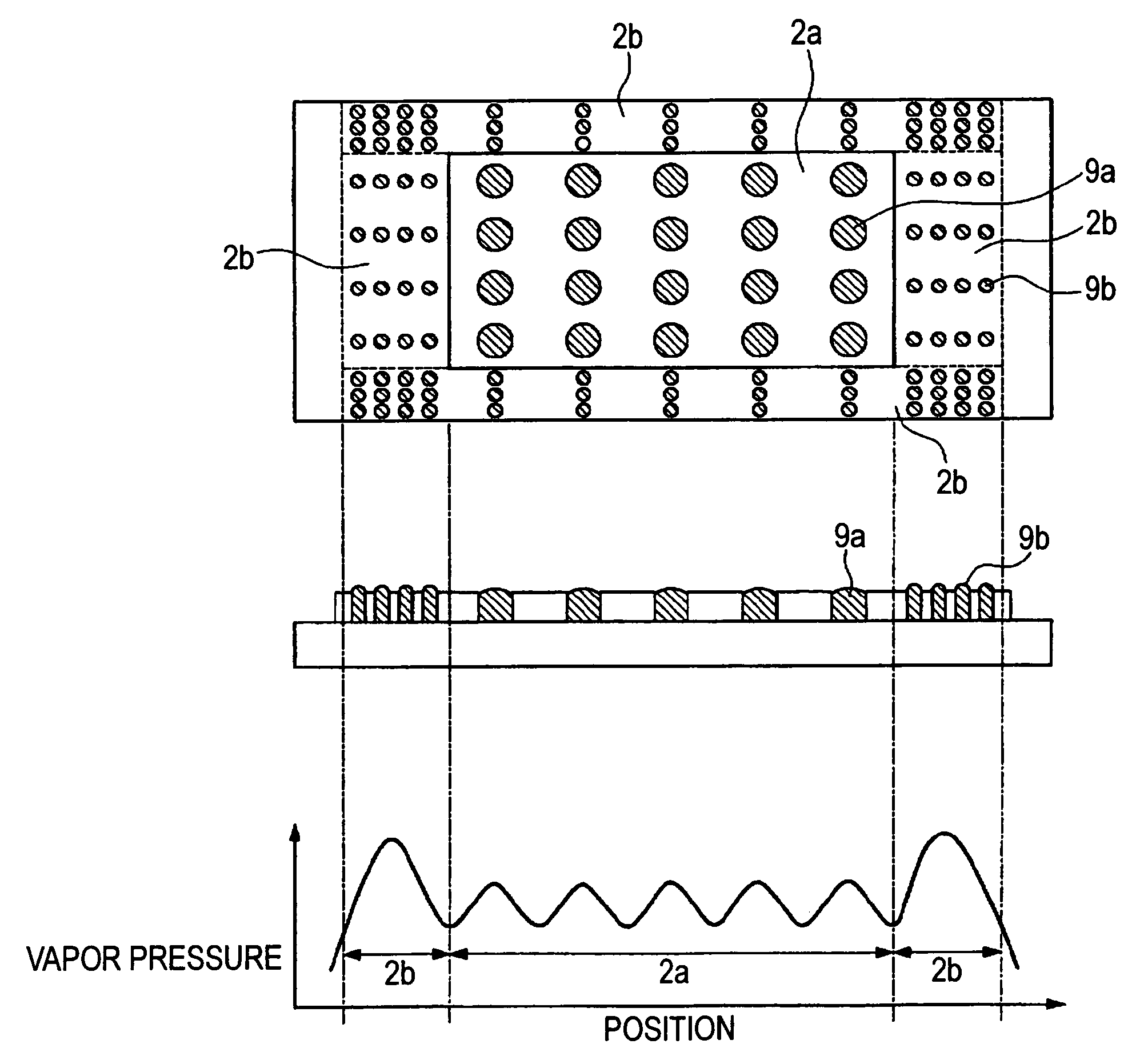
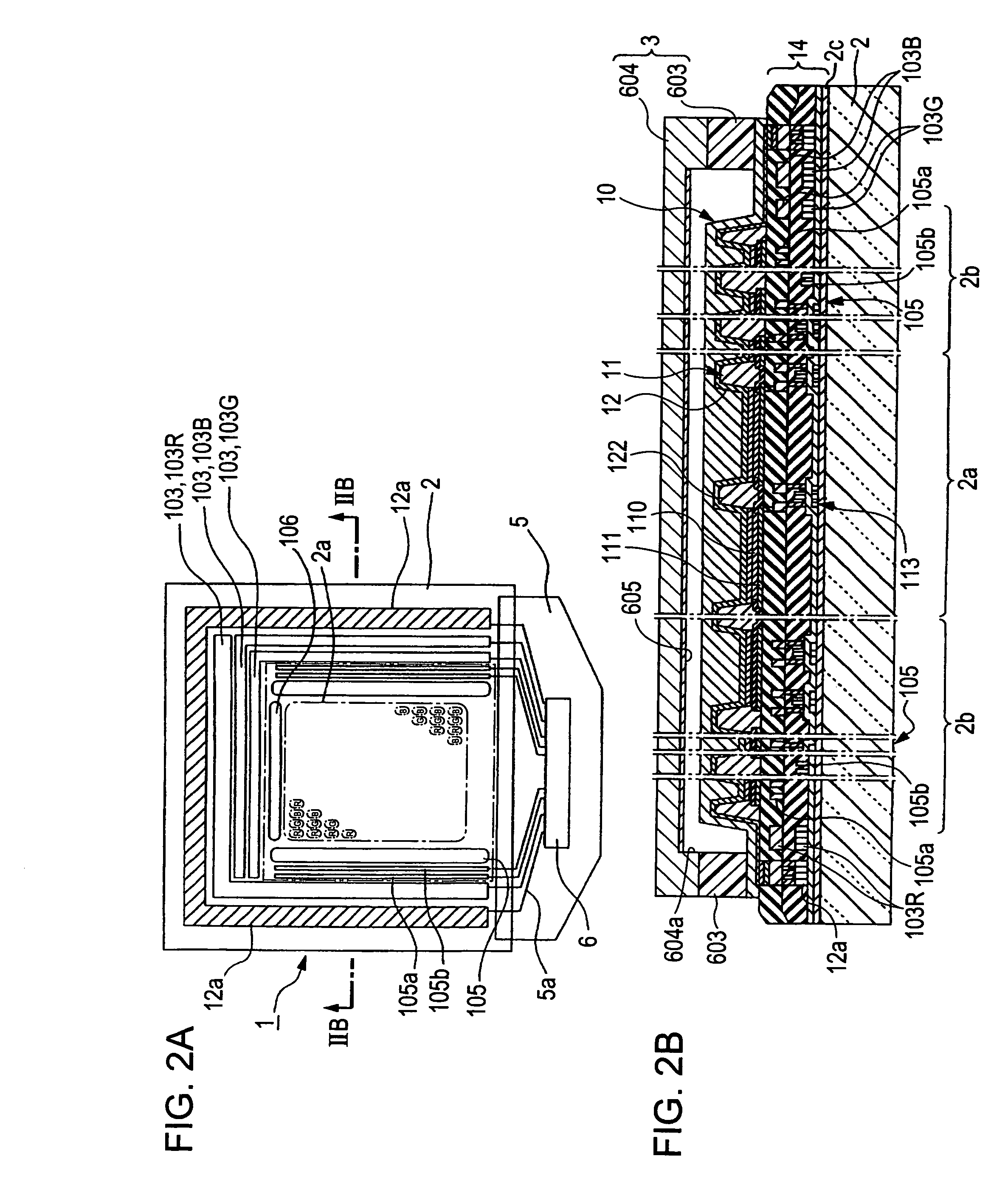
[0074]FIG. 1 is an explanatory view showing a wiring structure of an organic EL display device of the present embodiment. FIG. 2A is a plan view schematically showing the organic EL display device of the present embodiment and FIG. 2B is a cross-sectional view schematically showing the organic EL display device.

[0075]As shown in FIG. 1, the organic EL display device 1 of the present embodiment has a plurality of scanning lines 101, a plurality of signal lines 102 which extend in a direction to cross the scanning lines 101, and a plurality of power lines 103 which extend parallel to the signal lines 103. At intersections of the scanning lines 101 and the signal lines 102, pixel regions A are provided.

[0076]The signal lines 102 are connected to a data-side driving circuit 104 provided with a shift resister, a leve...

second embodiment

[0207]Next, an example of an electronic apparatus having the display device according to the first embodiment will be described. FIG. 30 is a perspective view showing an example of a cellular phone. In FIG. 30, reference numeral 600 denotes a cellular phone main body and reference numeral 601 denotes a display unit using the display device 1. Since such an electronic apparatus has the display unit using the display device 1 according to the first embodiment and characteristics of the display device 1, small irregularity of display and excellent display quality can be achieved.


PUM

PropertyMeasurementUnit
thicknessaaaaaaaaaa
thicknessaaaaaaaaaa
thicknessaaaaaaaaaa

Abstract

The color filter substrate has a functional region which includes a plurality of colored layers and which functions as a color filter selectively transmitting predetermined color light components and a non-functional region other than the functional region. The method includes discharging, onto a substrate, a liquid material, in which coloring materials constituting the colored layers are dissolved or dispersed into a solvent, with a liquid droplet discharge method. In the discharging of the liquid material, the liquid material is discharged onto the functional region and the liquid material or the solvent is discharged onto the non-functional region. The amount of the solvent discharged onto the non-functional region per unit area is larger than the amount of the solvent discharged onto the functional region per unit area.

Description

BACKGROUND OF THE INVENTION[0001]1. Technical Field[0002]The present invention relates to a method of manufacturing a color filter substrate, to a method of manufacturing an electro-optical device, to an electro-optical device, and to an electronic apparatus.[0003]2. Related Art[0004]Recently, an electro-optical device in which a functional layer made of a functional material is disposed between a pair of electrodes has been developed. In this case, in order to pattern the functional material, a liquid droplet discharge method in which the functional material, such as an organic fluorescent material, is made as ink and the resultant ink (composition) is discharged onto a base substrate is adopted. In particular, an organic electroluminescent (EL) device in which an organic light emitting material is used as the functional material has been developed.[0005]As the method of patterning the above-described functional material, a method is adopted in which a partition wall is formed arou...

Claims


Application Information

Patent Timeline
Patent Type & Authority Patents(United States)
IPC IPC(8): B05D5/06B05D5/12H01L21/00H01L21/77H01L21/84H01L27/00H01L27/32H01L51/00H01L51/40H01L51/52H01L51/56
CPCH01L27/3211H01L51/0005H01L21/67155H01L27/1214H01L27/3244H01L51/0007H01L51/0028H01L51/0096H01L51/5237H01L51/56H01L2251/5315H10K59/35H10K59/12H10K71/135H10K71/15H10K71/441H10K77/10H10K50/841H10K71/00H10K2102/3026H10K71/70F25D31/002B67D1/0042B67D2001/0095
Inventor KIMURA, HIDEYUKISEKI, SHUNICHIYAMAMOTO, NAOKI
Owner KATEEVA
Why Eureka
Try Eureka