Boron phosphide-based semiconductor device, production method thereof, light-emitting diode and boron phosphide-based semiconductor layer

a technology of boron phosphide and semiconductor layer, which is applied in the direction of polycrystalline material growth, polycrystalline material growth, crystal growth process, etc., can solve the problems of boron phosphide-based semiconductor layer containing twinning that light-emitting device having excellent emission intensity, for example, cannot be stably obtained, etc., to prevent the propagation of dislocation, reduce the density of dislocation, and improve the crystallinity

Inactive Publication Date: 2008-12-16
RESONAC HOLDINGS CORPORATION
View PDF4 Cites 6 Cited by
  • Summary
  • Abstract
  • Description
  • Claims
  • Application Information

AI Technical Summary

Benefits of technology

[0020]According to the present invention, as described above, since the boron phosphide-based semiconductor layer provided on the Si single crystal substrate is composed of a polycrystal layer that is an aggregate of single crystal entities containing twinning capable of absorbing misfit dislocation and preventing the propagation of dislocation, it is possible to construct a boron phosphide-based semiconductor layer excellent in crystallinity and reduced in the dislocation density. As a result, it is possible to provide a boron phosphide-based semiconductor device using the boron phosphide-based semiconductor layer and having excellent characteristics, such as high emission intensity, excellent rectification property and high breakdown voltage.
[0021]In addition, since the upper and lower clad layers sandwiching the light-emitting layer of the light-emitting diode according to the present invention are composed of the polycrystal layer that is an aggregate of a plurality of single crystal entities including the twining and since the lower clad layer is adjusted to have a thickness that can bring about emitted-light reflection of not less than 30%, it is possible to provide a light-emitting diode excellent in efficiency of taking out emitted light toward the outside.

Problems solved by technology

However, as disclosed in conventional techniques, the boron phosphide-based semiconductor layer containing twinning cannot be stably obtained.
That is, conditions necessary for producing a boron phosphide-based semiconductor layer stably containing twinning -are not heretofore clarified and therefore a light-emitting device having excellent emission intensity, for example, cannot be stably obtained.

Method used


Image

  • Boron phosphide-based semiconductor device, production method thereof, light-emitting diode and boron phosphide-based semiconductor layer
  • Boron phosphide-based semiconductor device, production method thereof, light-emitting diode and boron phosphide-based semiconductor layer
  • Boron phosphide-based semiconductor device, production method thereof, light-emitting diode and boron phosphide-based semiconductor layer

Examples


examples

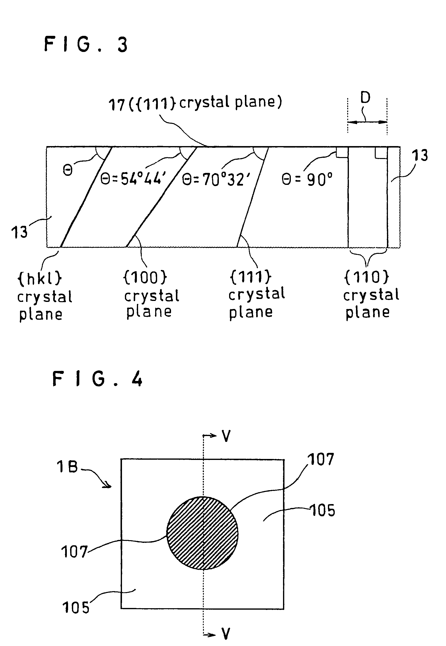
[0048]The present invention is described in more detail below with reference to a case where an LED is fabricated from a stacked layer structure comprising a {111}-Si single crystal substrate having provided thereon a boron phosphide (BP) layer comprising a polycrystal layer.

[0049]FIG. 4 is a schematic plan view of an LED 1B according to the present invention, and FIG. 5 a schematic cross section of the LED 1B taken along line V-V in FIG. 4.

[0050]In a stacked layer structure 1A for use in the LED 1B, a boron-doped p-type Si single crystal having a plane offset by 2° from the {111} plane was constructed as a substrate 101. On the substrate 101, a buffer layer 102 composed of boron phosphide mainly comprising an amorphous one in the as-grown state was deposited at 350° C. by an atmospheric-pressure MOCVD method using a triethylborane ((C2H5)3B) / phosphine (PH3) / hydrogen (H2) system. The thickness of the buffer layer 102 thus deposited was about 10 nm.

[0051]On the surface of the buffer ...


PUM

PropertyMeasurementUnit
angleaaaaaaaaaa
temperatureaaaaaaaaaa

Abstract

A boron phosphide-based semiconductor device enhanced in properties includes a substrate (11) composed of a {111}-Si single crystal having a surface {111} crystal plane and a boron phosphide-based semiconductor layer formed on the surface of the substrate and composed of a polycrystal layer (12) that is an aggregate of a plurality of a triangular pyramidal single crystal entities (13) of the boron phosphide-based semiconductor crystal, where in each single crystal entity has a twining interface that forms an angle of 60° relative to a <110> crystal direction of the substrate.

Description

CROSS REFERENCES TO RELATED APPLICATIONS[0001]This application is a National Stage of International Application No. PCT / JP03 / 00798 filed on Jan. 28, 2003, claiming priority based on Japanese Patent Application No. 2002-18188, filed Jan. 28, 2002 and Japanese Patent Application No. 2002-26271 filed Feb. 4, 2002 and claiming the benefit pursuant to §119(e)(1) of the filing date of Provisional Application Ser. Nos. 60 / 356,738 and 60 / 356,756, both filed Feb. 15, 2002 pursuant to 35 U.S.C. §111(b).TECHNICAL FIELD[0002]The present invention relates to a crystal structure of a boron phosphide-based semiconductor layer formed on a silicon (Si) single crystal (silicon) substrate, which is suitable for obtaining a boron phosphide-based semiconductor device, to a boron phosphide-based semiconductor device having the structure, to a method of producing the semiconductor device and to a light-emitting diode.BACKGROUND ART[0003]There are conventionally known techniques of forming by the use of bo...

Claims


Application Information

Patent Timeline
Patent Type & Authority Patents(United States)
IPC IPC(8): B32B17/06C30B23/00C30B25/00C30B28/12C30B28/14H01L21/00H01L21/28C30B25/02C30B29/40H01L21/20H01L21/205H01L29/04H01L29/201H01L33/02H01L33/16H01L33/30H01L33/50
CPCC30B25/02C30B29/40C30B29/403C30B29/406H01L21/02381H01L21/02461H01L21/02543H01L21/02579H01L21/02595H01L21/0262H01L29/045H01L29/201H01L33/02H01L33/30H01L33/16H01L33/18
Inventor UDAGAWA, TAKASHIYAMASHITA, TAMOTSU
Owner RESONAC HOLDINGS CORPORATION
Why Eureka
Try Eureka