Positioning of nanoparticles and fabrication of single electron devices

a single electron device and nanoparticle technology, applied in nanoinformatics, instruments, material analysis, etc., can solve the problems of stalled development of devices comprising sets, affecting the implementation of sets, and requiring precision geometric control at nanometer scal

Inactive Publication Date: 2008-12-16
BOARD OF RGT THE UNIV OF TEXAS SYST
View PDF1 Cites 156 Cited by
  • Summary
  • Abstract
  • Description
  • Claims
  • Application Information

AI Technical Summary

Benefits of technology

[0012]The single electron structure of the present invention is capable of taking advantage of complementary metal-oxide semiconductor (CMOS) technology. Compositions and methods of the present invention are compatible with CMOS materials and processes. The present invention may be fabricated using a structure comprising CMOS. The present invention may be incorporated into existing CMOS circuits.

Problems solved by technology

This is because a single electron device is inherently of nanoscale order and no current technique has been developed to fabricate such nanoscale elements at the wafer level.
To date, the requirement for geometric control with nanometer scale precision has stalled development of devices comprising SETs.
Additional fabrication issues have hindered the implementation of SETs.
Unfortunately, none of these techniques have been able to consistently control the gap between the source and drain electrodes at the wafer level.
Unfortunately, these techniques are unable to precisely control the positioning of charging islands and when scanning probes are used, the techniques are too slow for practical application.
The limitations have lead to the current inability to practically fabricate real and useful SETs at the wafer level.

Method used


Image

  • Positioning of nanoparticles and fabrication of single electron devices
  • Positioning of nanoparticles and fabrication of single electron devices
  • Positioning of nanoparticles and fabrication of single electron devices

Examples


Embodiment Construction

[0030]Although making and using various embodiments of the present invention are discussed in detail below, it should be appreciated that the present invention provides many inventive concepts that may be embodied in a wide variety of contexts. The specific aspects and embodiments discussed herein are merely illustrative of ways to make and use the invention, and do not limit the scope of the invention.

[0031]In the description which follows like parts may be marked throughout the specification and drawing with the same reference numerals, respectively. The drawing figures are not necessarily to scale and certain features may be shown exaggerated in scale or in somewhat generalized or schematic form in the interest of clarity and conciseness.

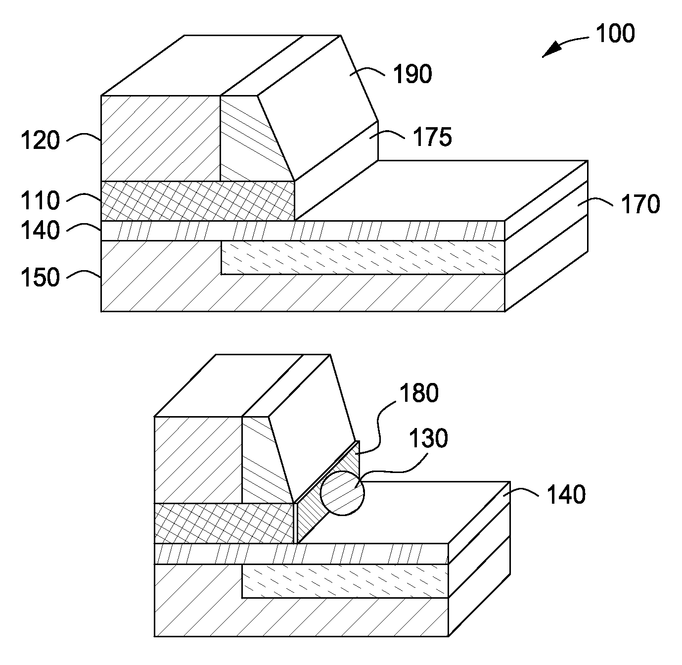
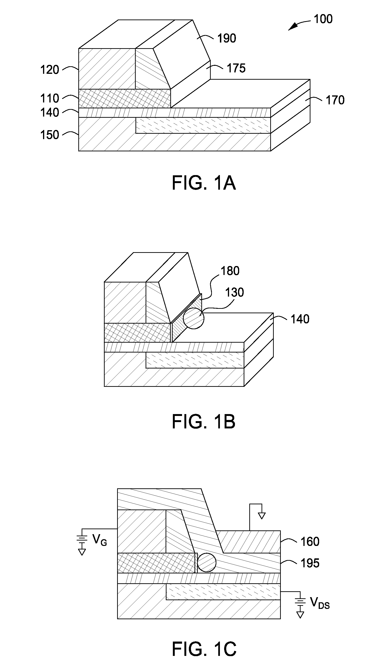
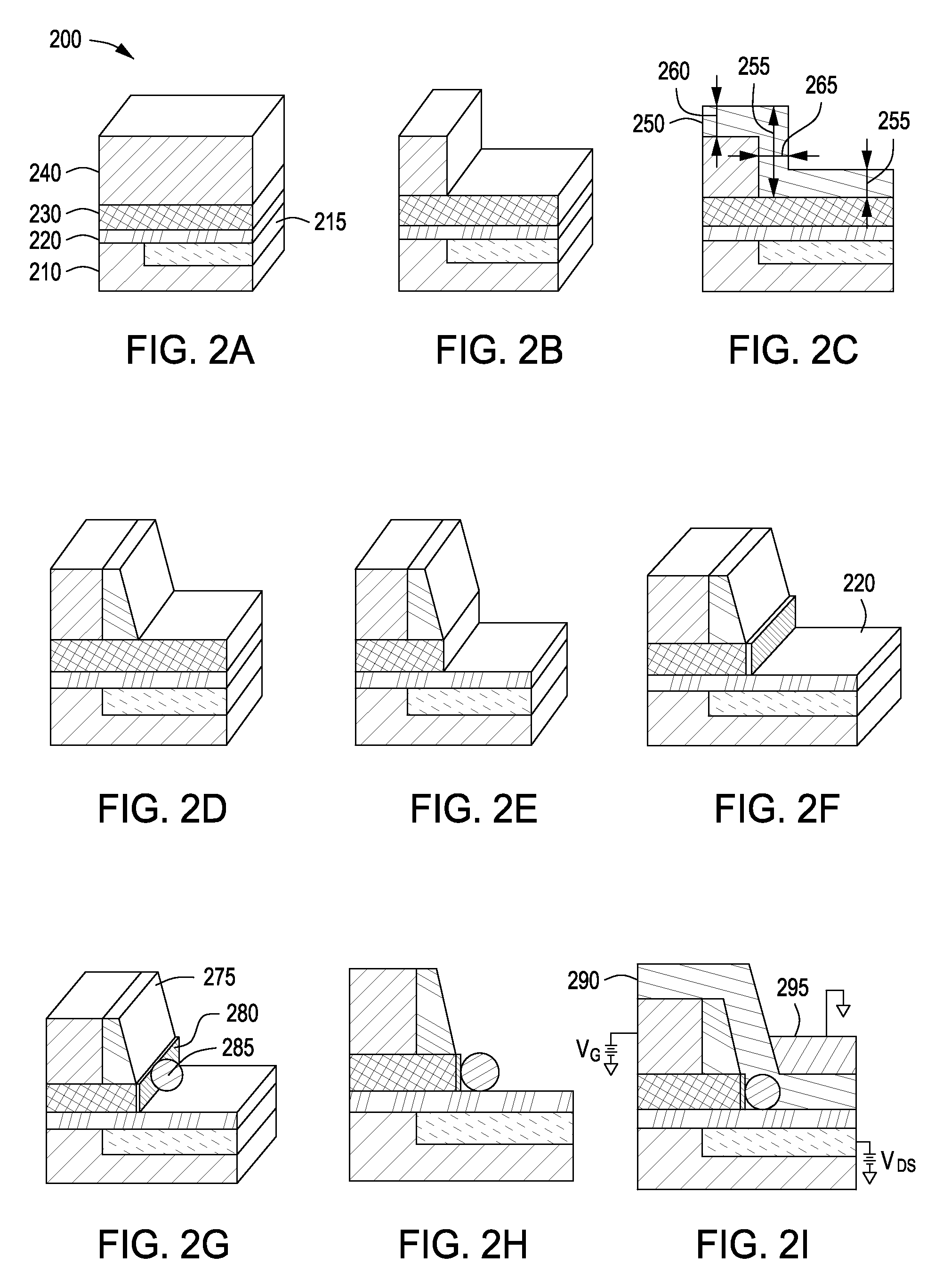
[0032]In general, the present invention takes advantage of some features of a single electron transistor (SET), the present invention comprising a single electron structure with a substrate having a surface and functioning with a source, a drain,...


PUM

PropertyMeasurementUnit
distanceaaaaaaaaaa
thicknessaaaaaaaaaa
thicknessaaaaaaaaaa

Abstract

The present invention includes single electron structures and devices comprising a substrate having an upper surface, one or more dielectric layers formed on the upper surface of the substrate and having at least one exposed portion, at least one monolayer of self-assembling molecules attracted to and in contact with the at least one exposed portion of only one of the one or more dielectric layers, one or more nanoparticles attracted to and in contact with the at least one monolayer, and at least one tunneling barrier in contact with the one or more nanoparticles. Typically, the single electron structure or device formed therefrom further comprise a drain, a gate and a source to provide single electron behavior, wherein there is a defined gap between source and drain and the one or more nanoparticles is positioned between the source and drain.

Description

CROSS-REFERENCES TO RELATED APPLICATIONS[0001]This application is a continuation of prior U.S. application Ser. No. 11 / 327,885 filed Jan. 9, 2006, herein incorporated by reference.BACKGROUND OF THE INVENTION[0002]The present invention relates to the field of electronics, and more specifically to the fabrication of single electron devices on a nanometer scale.[0003]With single electron technology, the transport of individual electrons should be precisely controlled. By operating with fewer electrons than current electronic devices, single electron technology makes it possible to fabricate extremely small electronic structures that offer several advantages, such as increasing sensitivity and conserving power, as examples.[0004]Although the potential benefit of single electron technology is clear, the fabrication and the reliable production of addressable structures and devices therefrom is in its infancy. This is because a single electron device is inherently of nanoscale order and no...

Claims


Application Information

Patent Timeline
Patent Type & Authority Patents(United States)
IPC IPC(8): H01L29/06H01L21/8234
CPCB82Y10/00G01N27/4146H01L21/28273H01L29/7613H01L29/7888H01L29/40114
Inventor KOH, SEONG JINKIM, CHOONG-UNMA, LIANG-CHIEHSUBRAMANIAN, RAMKUMAR
Owner BOARD OF RGT THE UNIV OF TEXAS SYST
Why Eureka
Try Eureka