Power module

a power module and power supply technology, applied in the field of power modules, can solve the problems of inability to reduce significantly, individual semiconductor chips are subject to a higher voltage load, and the inductance introduced into the module by each bond connection is relatively high, so as to improve the cooling effect of stacked semiconductor chips

Inactive Publication Date: 2008-12-16
SIEMENS AG
View PDF10 Cites 7 Cited by
  • Summary
  • Abstract
  • Description
  • Claims
  • Application Information

AI Technical Summary

Benefits of technology

[0014]This cuboid-shaped embodiment of the power module then allows at least one flat face of this power module to be provided with a heatsink, whereby direct cooling of the stacked semiconductor chips of the power module is achieved.

Problems solved by technology

These bonding wires have the following disadvantages however:The inductance introduced into the module by each bond connection is relatively high, whereby the individual semiconductor chips are subject to a higher voltage load during a switching action.
It is not possible to reduce significantly this parasitic inductance for geometric and fabrication reasons.The current density at the bonding point itself is relatively high, reducing the reliability of the connection.It is almost impossible to implement more complex topologies by this fabrication technique because of the crossover of bond connections.

Method used


Image

  • Power module
  • Power module
  • Power module

Examples


Embodiment Construction

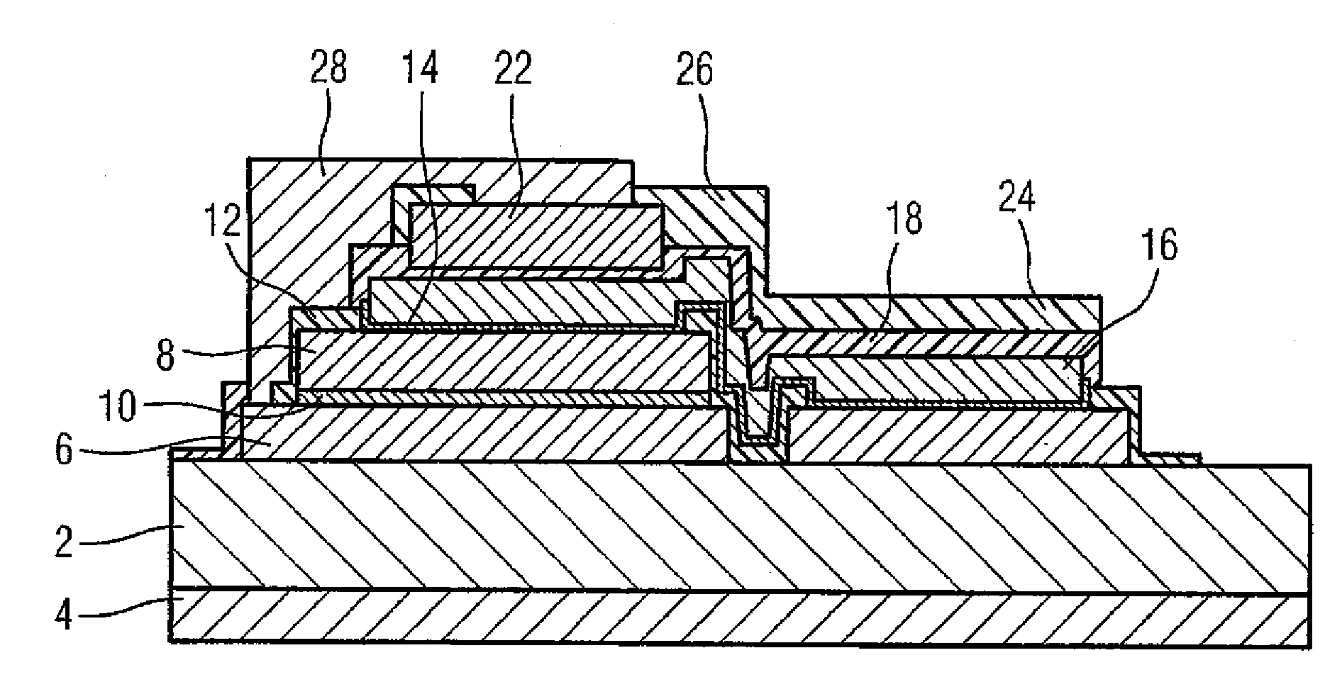
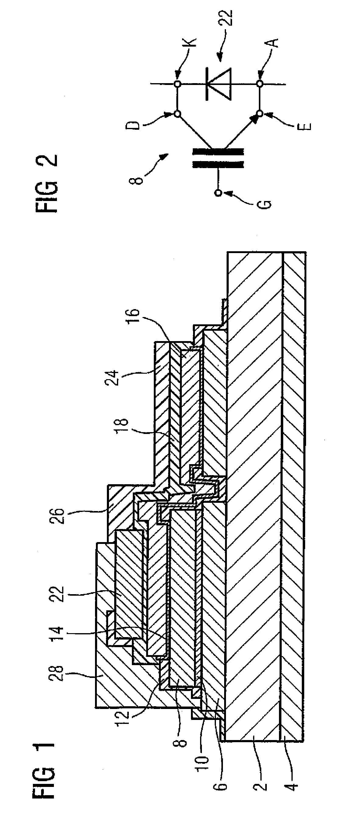
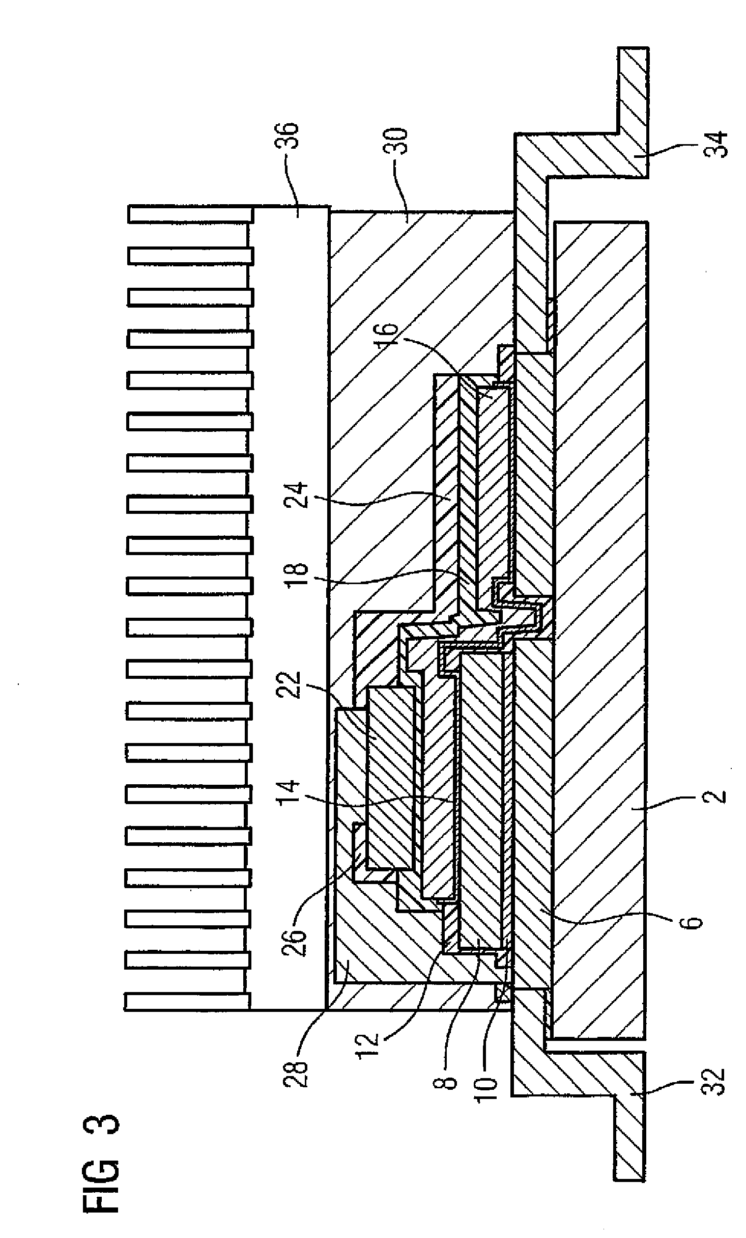
[0024]In FIG. 1, 2 denotes a substrate, 4 denotes a lower electrically conducting layer, 6 an upper electrically conducting layer and 8 a semiconductor chip. This semiconductor chip 8 is an active semiconductor chip, in particular a switchable semiconductor chip. An Insulated Gate Bipolar Transistor chip (IGBT) is used as the switchable semiconductor chip, for example. These electrically conducting layers 4 and 6 are made of copper. A layer 10 made of soft solder is arranged between the semiconductor chip 8 and the upper electrically conducting layer 6 of the substrate 2. A film 12 made of an electrically insulating material lies in close contact with the surfaces of the substrate 2, of the upper electrically conducting layer 6 and of the semiconductor chip 8. To enable contact to be made with the upper contacts (emitter and gate contact E and G) of the semiconductor chip 8, this film 12 has a window 14, which exposes these contact surfaces of the upper contacts of the semiconductor...


PUM


Abstract

The invention relates to a power module comprising a substrate (2), whose surfaces are provided with at least one electrically conductive layer (4, 6), at least one active semiconductor chip (8), which is electrically connected to an electrically conductive layer (6), a film (12) consisting of an electrically conductive material, which is in close contact with the surfaces of the semiconductor chips (8) of the electrically conductive layer (6) and the substrate (2) and is provided with planar printed conductors (16). According to the invention: the module is equipped with a second film (18), which is in close contact with the surfaces of the printed conductors (16) and the first film (12); a passive semiconductor chip (22) is applied to said second film (18), above the active semiconductor chip (8) and is electrically connected to the planar printed conductor (16) lying below by means of a window (14) that is configured in the second film (18); the module is equipped with a third film (24), which is in close contact with the surfaces of the passive semiconductor chip (22) and the second film (18) and said third film (24) is provided with a planar printed conductor (28), which is conductively connected to the conductive layer (6) lying below the active semiconductor chip (8). The invention thus provides a compact power module that can comprise complex topologies.

Description

BACKGROUND OF THE INVENTION[0001]The invention relates to a power module.[0002]Power electronic components such as switchable semiconductors and diodes are often combined in power modules in order to implement certain topologies such as pulse converters and / or power rectifiers in one module. The individual components in such a module are connected by bonding wires that lead from one power component, for example a switchable semiconductor chip, in particular an Insulated Gate Bipolar Transistor chip (IGBT), to another power component, for example a diode chip, or to a printed conductor on a substrate of this power module.[0003]These bonding wires have the following disadvantages however:[0004]The inductance introduced into the module by each bond connection is relatively high, whereby the individual semiconductor chips are subject to a higher voltage load during a switching action. It is not possible to reduce significantly this parasitic inductance for geometric and fabrication reas...

Claims


Application Information

Patent Timeline
Patent Type & Authority Patents(United States)
IPC IPC(8): H01L23/02H01L21/60H01L23/538H01L25/07H01L25/18
CPCH01L23/5389H01L24/24H01L24/82H01L25/071H01L25/18H01L2924/1305H01L2224/2402H01L2224/24051H01L2224/24226H01L2224/24998H01L2224/32145H01L2924/01004H01L2924/0101H01L2924/01013H01L2924/01029H01L2924/01032H01L2924/01052H01L2924/01075H01L2924/01082H01L2924/13055H01L2924/30107H01L2924/01019H01L2924/01033H01L2924/01068H01L2924/014H01L2224/82007H01L2924/00H01L2924/181H01L2224/32225H01L2924/00012
Inventor ECKARDT, DIETERREBBEREH, CARSTEN
Owner SIEMENS AG
Why Eureka
Try Eureka