Wired circuit board for controlling characteristic impedances of a connection terminal
a technology of characteristic impedances and connection terminals, which is applied in the direction of laminating printed circuit boards, high-frequency circuit adaptations, instruments, etc., can solve the problems of unavoidable reduction in transmission efficiency at the connection point, inability to control characteristic impedances at the connection points between read wires and write wires, and reduced signal transmission efficiency. , to achieve the effect of improving signal transmission efficiency and reducing capacitan
- Summary
- Abstract
- Description
- Claims
- Application Information
AI Technical Summary
Benefits of technology
Problems solved by technology
Method used
Image
Examples
example 1
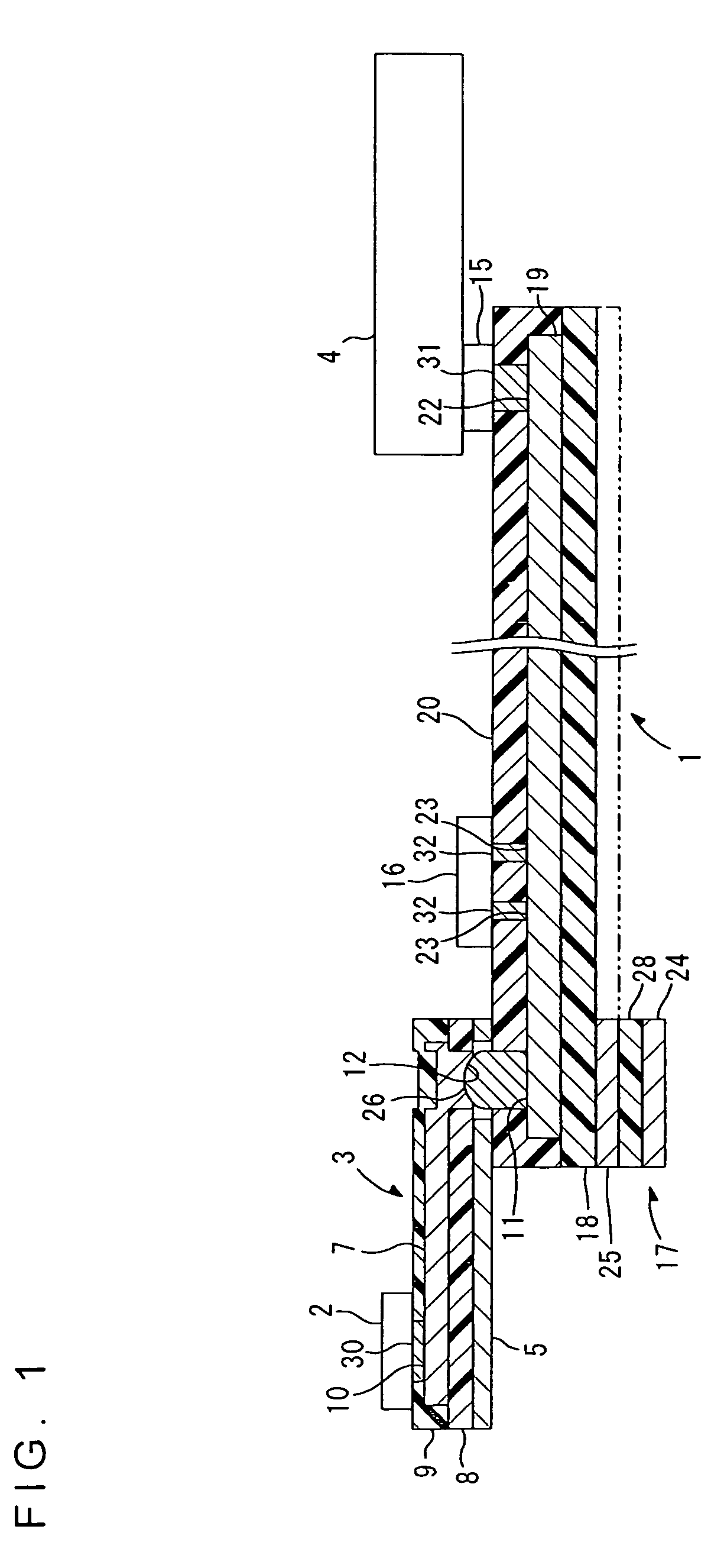
[0071]A double-sided copper clad laminate (ESPANEX (product name) available from Nippon Steel Chemical Co., Ltd.) having a copper foil having thickness of 12.5 μm on each side of polyimide sheet having thickness of 12.5 μm was prepared.
[0072]After the double-sided copper clad laminate was covered with a dry film photoresist, the dry film photoresist was exposed to light and then developed to form it into a resist pattern to cover a wired-circuit-pattern forming portion and a conductive-board forming portion.
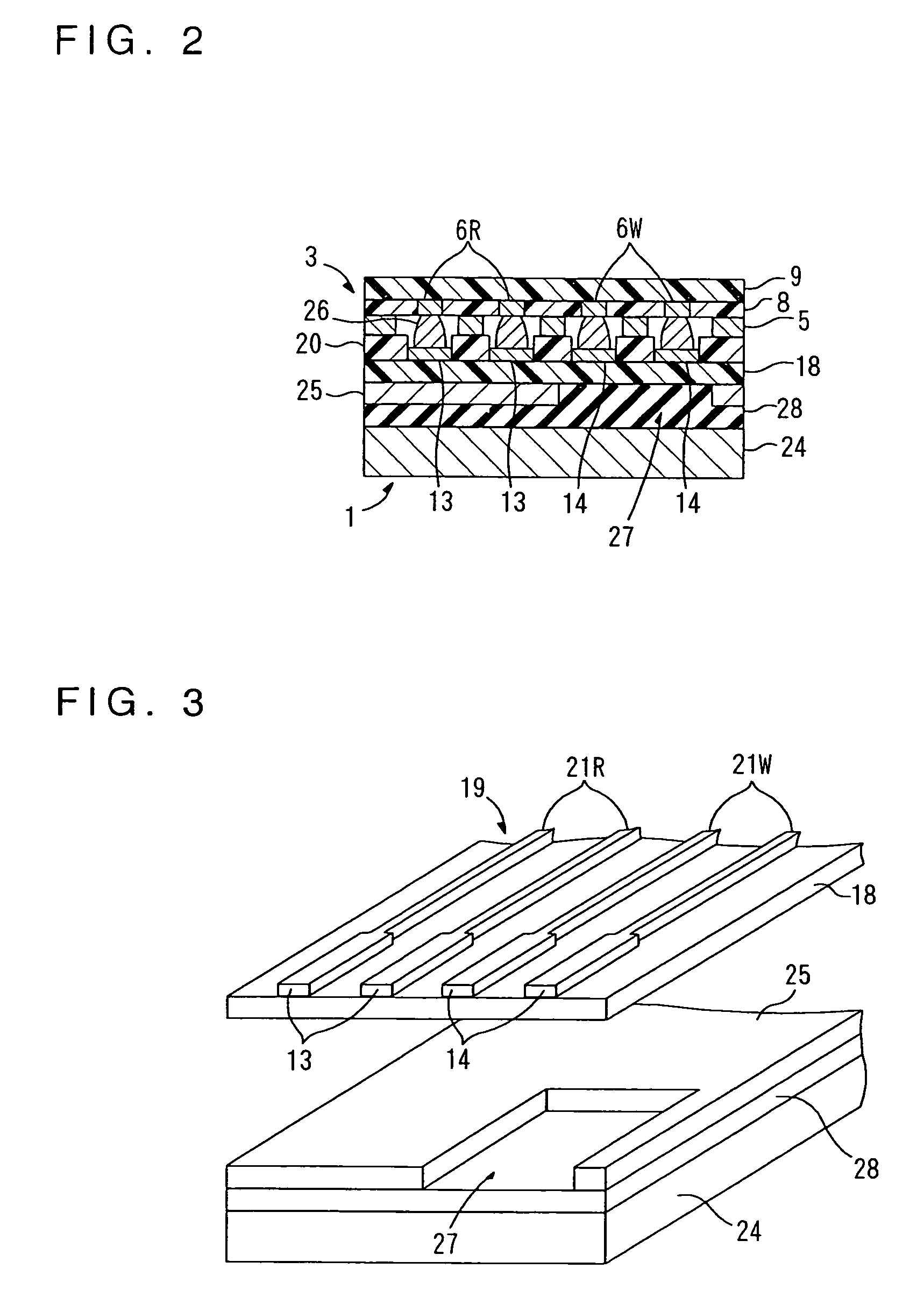
[0073]Then, after the copper foil exposed from the resist was etched, the resist was removed, thereby forming, on one side of the polyimide sheet, the conductor layer of the wired circuit pattern having the read lines and the write lines having the first terminal portions and the second terminal portions, respectively, and also forming, on the other side of the polyimide sheet, the conductive board having at a portion thereof the opening overlapping with the second terminal porti...
example 2
[0075]A single-sided copper clad laminate (ESPANEX (product name) available from Nippon Steel Chemical Co., Ltd.) having a copper foil having thickness of 12.5 μm on one side of polyimide sheet having thickness of 12.5 μm was prepared.
[0076]After the single-sided copper clad laminate was covered with a dry film photoresist, the dry film photoresist was exposed to light and then developed to form it into a resist pattern to cover a wired-circuit-pattern forming portion.
[0077]Then, after the copper foil exposed from the resist was etched, the resist was removed, thereby forming, on one side of the polyimide sheet, the conductor layer of the wired circuit pattern having the read lines and the write lines having the first terminal portions and the second terminal portions, respectively.
[0078]Thereafter, a generally rectangular aluminum sheet of 100 μm thick having, at a portion thereof opposed to the second terminal portions, an opening previously formed by punching was adhesively bonde...
PUM
| Property | Measurement | Unit |
|---|---|---|
| distance | aaaaa | aaaaa |
| distance | aaaaa | aaaaa |
| thickness | aaaaa | aaaaa |
Abstract
Description
Claims
Application Information
 - R&D
- Intellectual Property
- Life Sciences
- Materials
- Tech Scout
- Unparalleled Data Quality
- Higher Quality Content
- 60% Fewer Hallucinations
Browse by: Latest US Patents, China's latest patents, Technical Efficacy Thesaurus, Application Domain, Technology Topic, Popular Technical Reports.
© 2025 PatSnap. All rights reserved.Legal|Privacy policy|Modern Slavery Act Transparency Statement|Sitemap|About US| Contact US: help@patsnap.com


