
Voltage level shifter

Active Publication Date: 2008-12-23
XILINX INC
View PDF6 Cites 51 Cited by
  • Summary
  • Abstract
  • Description
  • Claims
  • Application Information

AI Technical Summary

Benefits of technology

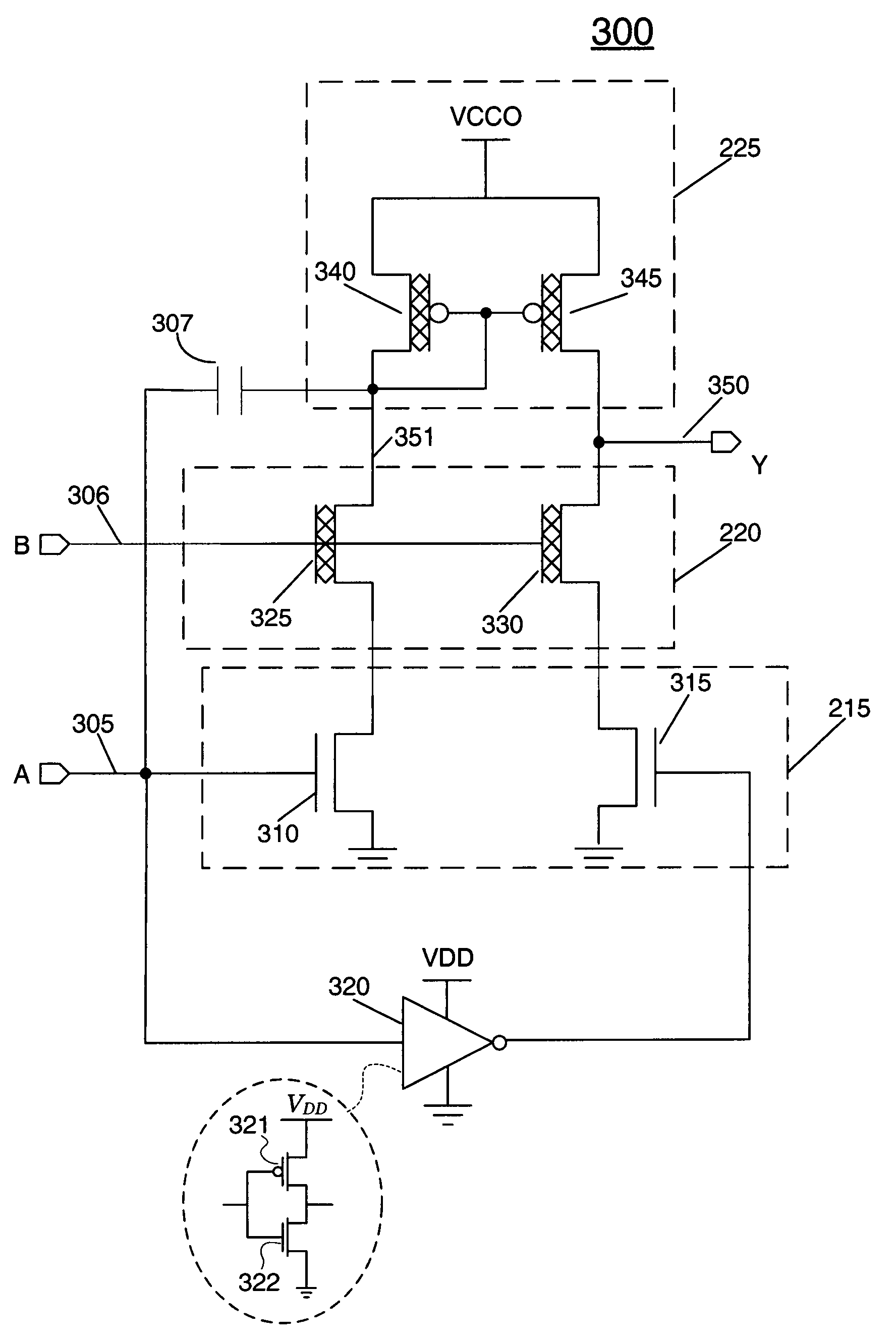
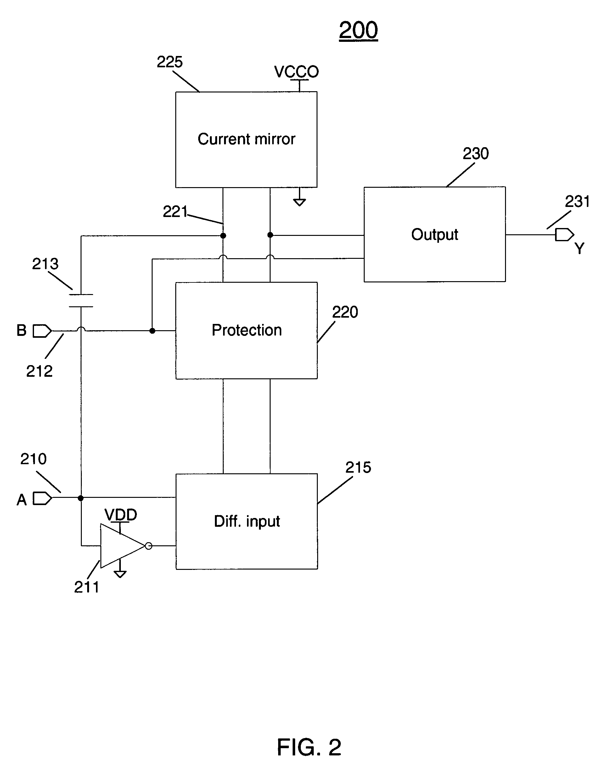
[0008]In accordance with embodiments of the present invention, a level shifter circuit includes a protection stage, a current mirror stage, and an input stage which may be coupled to input controls. The level shifter can maintain performance over wide range of power supplies voltages and I / O operating frequencies. The protection stage may be coupled between the current mirror stage and the input stage. The protection stage can isolate transistors receiving input signals at low voltage ranges from transistors driving output signals at high voltage ranges. A capacitor may be coupled between the input stage and a branch of the current mirror stage that may allow the level shifter to maintain performance at high frequencies.

Problems solved by technology

One of the challenges in designing ICs is to accommodate several different power supply voltages on a single IC.
A problem with prior art level shifters is that their performance can be highly dependent on certain factors, including I / O signals voltage levels, power supplies voltage ranges, and the I / O operating frequencies.
These factors may have a significant adverse effect on the performance of the level shifter, especially in a low voltage, and high-speed designs.

Method used


Image

  • Voltage level shifter
  • Voltage level shifter
  • Voltage level shifter

Examples


Embodiment Construction

[0016]The present invention is believed to be applicable to a variety of systems and integrated circuits (ICs). While the present invention is not so limited, an appreciation of the present invention is presented by way of specific examples. In the following description, numerous specific details are set forth to provide a more thorough understanding of the present invention. However, it will be apparent to one ordinarily skilled in the art that the present invention can be practiced without the specific details.

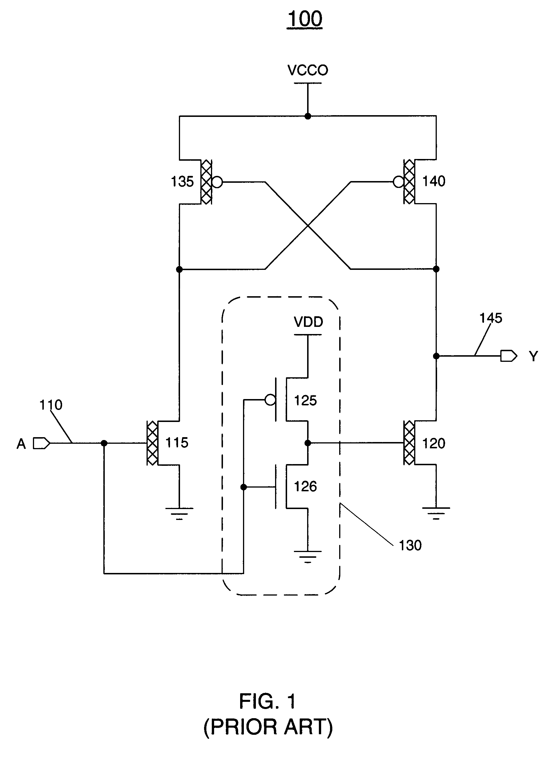
[0017]FIG. 1 shows a circuit diagram of a typical level shifter 100. The level shifter 100 includes NMOS transistors 115 and 120, PMOS transistors 135 and 140, and inverter 130. Transistors 115, 120, 135, and 140 are thick oxide transistors, while transistors 125 and 126, which form the inverter 130, are thin oxide transistors. Their thicker gate oxide allows transistors 115, 120, 135, and 140 to tolerate the greater voltages that may be supplied by a high voltage supply.

[00...


PUM


Abstract

A high-speed, area-efficient level shifter includes transistors having a variety of oxide thicknesses. The level shifter has a protection circuit stage, and a current mirror stage that allows the level shifter to perform over a wide voltage range at a high frequency. The level shifter maintains rise time, fall time, and duty cycle over a wide range of input and output voltage levels.

Description

FIELD OF THE INVENTION[0001]The invention relates to integrated circuits (ICs), and more particularly, to voltage level shifter circuits in ICs.BACKGROUND OF THE INVENTION[0002]Integrated circuits (ICs) which operate in two or more power supply voltages environment invariably require signals to interface between circuits supplied by different power supply voltages. One of the challenges in designing ICs is to accommodate several different power supply voltages on a single IC. Typically, an IC will have an internal or a core supply voltage used for powering the bulk of its internal circuitry. The voltage level of the internal supply is usually kept as low as possible in order to minimize power consumption and in some examples, to adhere to process node requirements. As IC fabrication processes continue to shrink the feature size of transistors, the ICs will continue to decrease in size, and therefore the allowable internal power supply voltage also decreases. For example, ICs fabrica...

Claims


Application Information

Patent Timeline
IPC IPC(8): H03K19/094H03K19/0175H03L5/00
CPCH03K19/00315H03K19/018528
Inventor TAN, JIANZHANG, QI
Owner XILINX INC
Learn More