
Method and device for driving liquid crystal on silicon display systems

a liquid crystal display and liquid crystal technology, applied in the field of driving mechanisms for liquid crystal on silicon display, can solve the problems of not meeting one or more of the challenges of most liquid crystal devices disclosed in the art, prone to a particular class of problems, and not providing the flexibility needed, so as to slow down the dc balancing rate, and reduce the possibility of dc offset effects and image sticking problems

Inactive Publication Date: 2008-12-23
GOOGLE LLC
View PDF11 Cites 22 Cited by
  • Summary
  • Abstract
  • Description
  • Claims
  • Application Information

AI Technical Summary

Benefits of technology

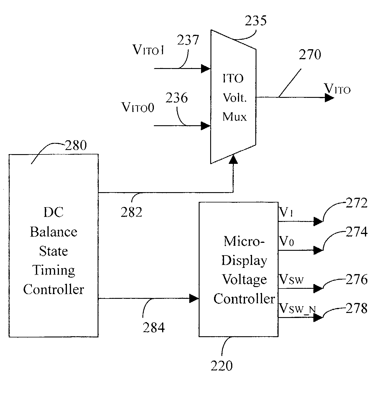
The present invention provides a pixel display configuration with a voltage controller in each pixel control circuit for controlling the voltage inputted to the pixel electrodes. This controller has a function of multiplexing the voltage input to the pixel electrodes and also a bit buffering and decoupling function to decouple and flexible change the input voltage level to the pixel electrodes. This invention increases the rate of DC balancing to one KHz and higher to mitigate the possibility of DC offset effects and image sticking problems caused by slow DC balancing rates. The invention also allows for switching from one DC balance state to another without rewriting the data onto the panels, which solves the problem of applying high voltage CMOS designs. The disclosures in this invention provide solutions to overcome the technical problem of slow DC balancing rates and high production cost and yield limitations of CMOS technologies.

Problems solved by technology

Liquid crystal on silicon (LCOS) microdisplay technology is still challenged by the need to DC balance the liquid crystal material accurately while generating images that are free of flicker and while limiting the RMS voltages to the useful range of the electro-optic efficiency curve of the liquid crystal device.
Most liquid crystal devices disclosed in the art fail to meet one or more of these challenges.
Each is prone to a particular class of problems.
All are prone to some degree to the related problems of DC offset and image flicker.
However, the conventional multiplexing devices that attempt to narrow the range of voltages that are applied to the pixel electrode on an instantaneous basis and that receive input signals directly from a memory cell fail to provide the needed flexibility because they are not capable of independently controlling the memory state that gets driven through the multiplexer to the pixel mirror.
Limited by these technical difficulties, the conventional technologies of LCOS display are provide displays of higher quality only with difficulty.
Specifically, the displays are often hindered by problems of image sticking and flicker due to the low DC balancing rates as will be further explained below.
As the cost of LCD systems continues to fall, i.e., is predicted that they will eventually take over the market for traditional CRT applications.
The biggest disadvantages of current CRT systems are their bulky size, geometry, and weight, as well as their high power consumption.
These disadvantages are clearly evident when comparing the features of CRT and LCD projection displays with similar characteristics.
However, the inherent physical characteristics of liquid crystal materials cause deterioration in the performance of the liquid crystal material due to an ionic migration or “drift” when a DC voltage is applied to them.
This will result in the contaminants plating out onto the alignment layer with the result in that the liquid crystal material will begin to “stick” at an orientation and not respond fully to the drive voltages.
This effect is manifested by the appearance of a ghost image of the previous image that is objectionable to viewers.
Known modulation schemes are not able to prevent liquid crystal deterioration while still being able to accurately control the RMS voltage as that applied to the liquid crystal in many projection applications where the display device is subjected to high heat loading and high light intensity.
In this case the display is extremely sensitive to ionic contamination because the charge on the pixel electrode will bleed off quickly and the display will flicker if such ionic contamination is present.
It follows that RMS voltages outside of this range are not useful and will cause gray scale distortions if applied to the crystal pixels.
Many known display systems drive the logic circuitry with voltages that are outside of the useful range of the liquid crystal, and applying these voltages directly onto the pixel electrode results in. wasted power.
But since the entire panel is written with voltage scales that alternate between a higher voltage range and a lower voltage range, conventional multiplexing devices fail to provide the needed flexibility because they are not capable of independently controlling the memory state that gets driven through the multiplexer to the pixel mirror.
This adds substantially to the complexity of the device because the modulated voltage must be correct in all respects as these same voltages are used to drive the pixel mirrors and thus achieve DC balance.
Design of a line that cam propagate a number of different voltages across long lines that must accurate in all cases is a significant design constraint.
All these technical difficulties limit the effectiveness of the above inventions in providing practical solutions to the above-mentioned limitations.
Furthermore, since the conventional systems utilize the state of the memory cell as a control signal to direct a voltage onto the pixel mirror, there is no independent means for selecting and directing a narrower range of voltages to be consistent with the electro-optical response curve, onto the pixel electrode.
It often leads to further difficulties and limitations.
Such approach places several limitations on the device: First, the common plane (VCOM) must be a fixed value because during the transition time data is present on the display in both upper and lower voltage ranges.
However, with this voltage range, there are very few liquid crystal materials available to satisfy the requirement of the panel.
For these reasons, manufacturing LCOS display panels and other LCD devices often results in a lower yields than average yield rate.
Thus, the production costs are increased when non-standard CMOS processes have to be carried out for manufacturing the LCOS device in order to satisfy these operational conditions when suitable liquid crystal materials are used.
Furthermore the technique of applying a DC balance switching rate of once per data load in the conventional micro-displays further creates a situation where the ion migrating within the liquid crystal material begin to plate out toward the end of the data frame at a lower DC balancing rate.
It is objectionable and in fact is a specification item for TFT displays that the old data must dissipate within a specified short period.
With a low DC balancing rate, a LCOS display often generates a second objectionable flicker artifact due to slow data rates caused by the existence of DC offset mechanisms.
This second problem creates a dilemma between solving flicker and eliminating image sticking.

Method used


Image

  • Method and device for driving liquid crystal on silicon display systems
  • Method and device for driving liquid crystal on silicon display systems
  • Method and device for driving liquid crystal on silicon display systems

Examples


Embodiment Construction

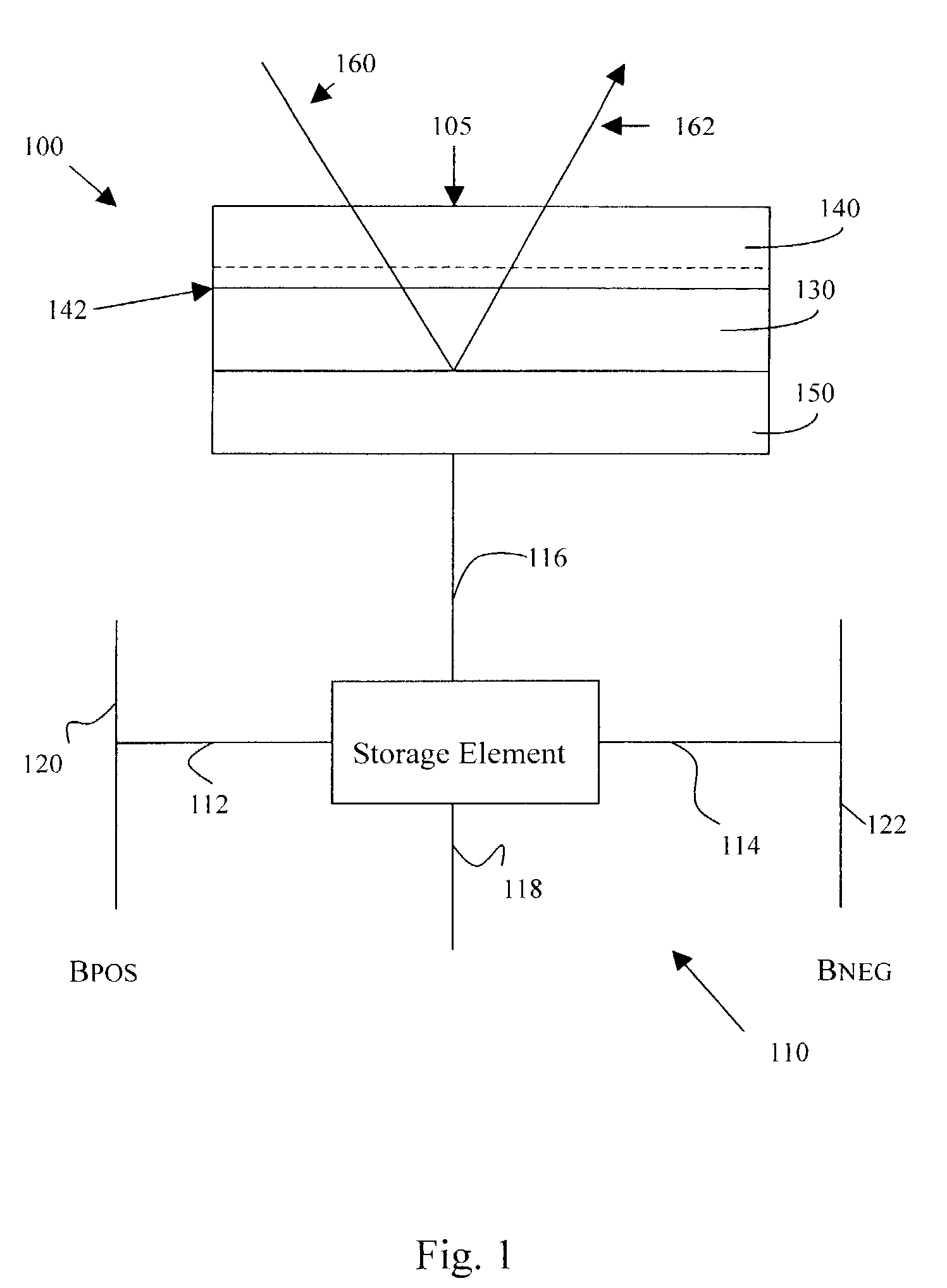
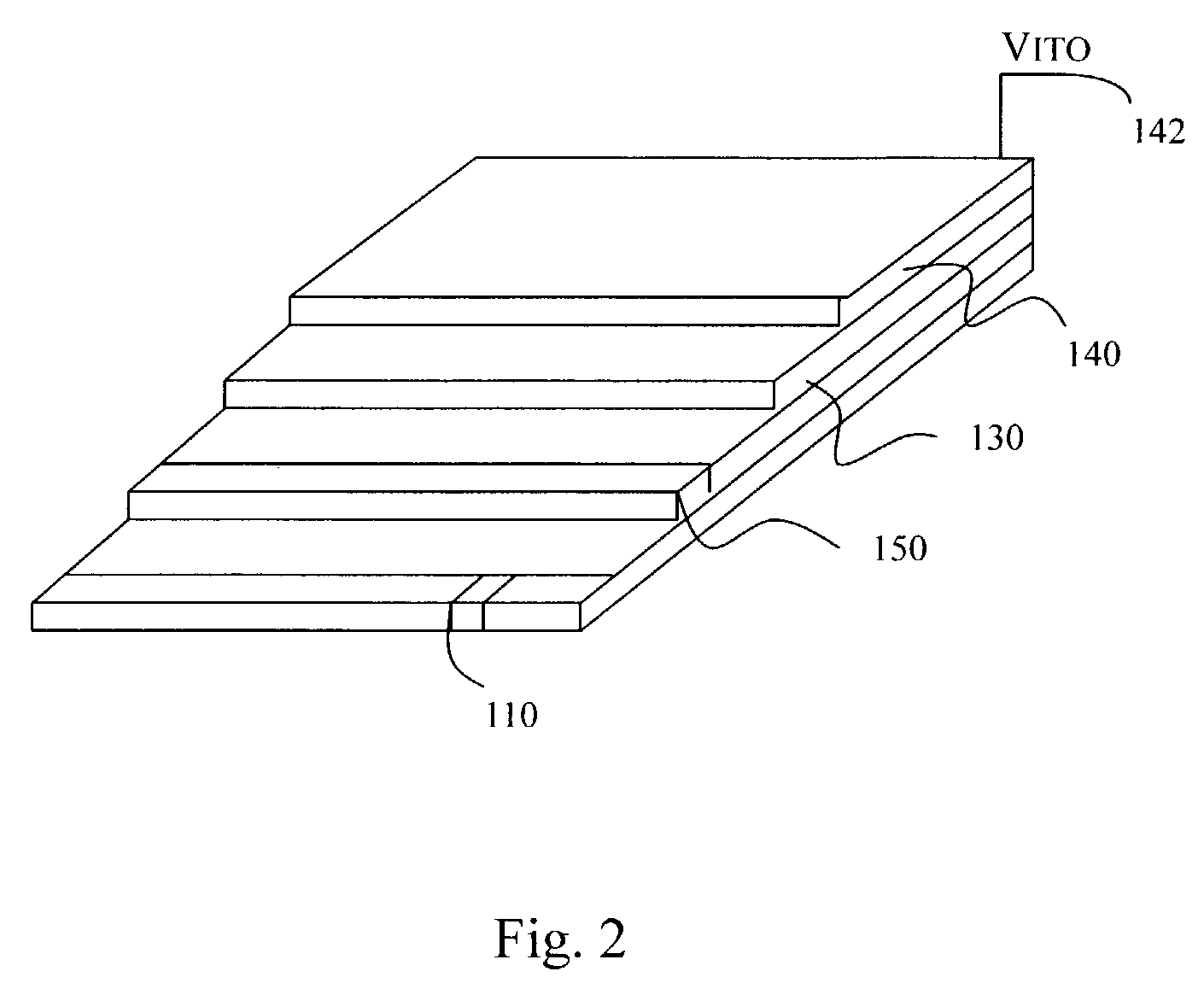
[0037]FIGS. 1 and 2 show the general construction of a liquid crystal on silicon (LCOS) micro-display panel 100. A single pixel cell 105 includes a liquid crystal layer 130 in between a transparent common electrode 140, and a pixel electrode 150. A storage element 110 is coupled to the pixel electrode 150, and includes complementary data input terminals 112 and 114, a data output terminal 116, and a control terminal 118. The storage element 110 is responsive to a write signal placed on control terminal 118, reads complementary data signals asserted on a pair of bit lines (BPOS and BNEG) 120 and 122, and latch the data signal through the output terminal 116. Since the output terminal 116 is coupled to the pixel electrode 150, the data (i.e. high or low voltage) passed by the storage element 110 is imparted on the pixel electrode 150. The pixel electrode 150 is preferably formed from a highly reflective polished aluminum. In the LCD display panel in accordance with the present inventi...


PUM


Abstract

The present invention discloses a pixel display configuration by providing a voltage controller in each pixel control circuit for controlling the voltage inputted to the pixel electrodes. The controller includes a function of multiplexing the voltage input to the pixel electrodes and also a bit buffering and decoupling function to decouple and flexible change the input voltage level to the pixel electrodes. The rate of DC balancing can be increased to one KHz and higher to mitigate the possibility of DC offset effects and the image sticking problems caused by slow DC balancing rates. This invention further discloses an enabling technology for switching from one DC balance state to another without rewriting the data onto the panels. Therefore, it is not required to implement a high voltage CMOS designs and standard CMOS technologies can be applied to manufacture the storage cells and control panel for the LCOS displays with lower production cost and higher yields.

Description

BACKGROUND OF THE INVENTION[0001]1. Field of the Invention[0002]The present invention pertains to liquid crystal on silicon (LCOS) displays, and more particularly to driving mechanisms for liquid crystal on silicon displays.[0003]2. Description of the Prior Art[0004]Liquid crystal on silicon (LCOS) microdisplay technology is still challenged by the need to DC balance the liquid crystal material accurately while generating images that are free of flicker and while limiting the RMS voltages to the useful range of the electro-optic efficiency curve of the liquid crystal device. Most liquid crystal devices disclosed in the art fail to meet one or more of these challenges. The current LCOS devices may be thought of as being divided into three classes, based on the method of creating grayscale. Each is prone to a particular class of problems. The three classes of devices are analog drive, digital drive based on simple SRAM, and complex digital drive. All are prone to some degree to the re...

Claims


Application Information

Patent Timeline
Patent Type & Authority Patents(United States)
IPC IPC(8): G09G5/00G09G3/36
CPCG09G3/3659H04N9/312G09G3/3614G09G3/3655G09G2300/0809G09G2300/0823G09G2300/0857G09G2320/0204G09G2320/0247
Inventor HUDSON, EDWIN LYLE
Owner GOOGLE LLC
Learn More