

Stress profile modulation in STI gap fill
a stress profile and gap filling technology, applied in the field of high density plasma (hdp) deposition techniques, can solve the problems of reducing the effective mass of electrons, consuming too much thermal budget for advanced transistor architectures, and affecting the efficiency of transistor fabrication processes, so as to achieve the effect of not adversely affecting the efficiency of the transistor fabrication process
Inactive Publication Date: 2009-01-27
NOVELLUS SYSTEMS
View PDF119 Cites 21 Cited by
- Summary
- Abstract
- Description
- Claims
- Application Information
AI Technical Summary
Benefits of technology
[0007]The present invention addresses this need by providing methods for forming silicon oxide films using high density plasma (HDP) CVD techniques. The methods can be used to tailor stress in deposited dielectric films in transistor architectures to generate and modulate channel strain without adversely impacting the efficiency of the transistor fabrication process.
Problems solved by technology
This renders it more difficult for the electrons to be ‘scattered’ between the lowest energy states by a phonon, because there are only two states to occupy.
Also, distorting the lattice through tensile strain can distort the electron-lattice interaction in a way that reduces the electron's effective mass, a measure of how much it will accelerate in a given field.
However, highly tensile silicon nitride capping layers are generally deposited using thermal CVD processes, which may consume too much of thermal budget for advanced transistor architectures.
In addition, silicon nitride capping layers are not appropriate for use in PMOS structures where it is preferable to have compressive strain in the PMOS channel region.
Additionally, biaxial strained silicon may also be achieved through the deposition of Si and silicon germanium (SiGe) epilayers, but is a costly process.
Method used
View moreImage
Smart ImageViewing Examples

Examples
example
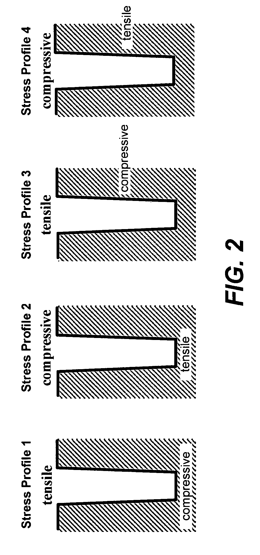
[0069]A series of HDP CVD SiO2 layers were deposited with conditions progressively changed to generate compressive to tensile stress in the resulting composite film. For layer 1, no backside He flow was used and the wafer temperature exceeded 400° C. Six additional layers were applied on the first layer with stepwise increases in the backside He pressure as follows: Layer 2, 1 Torr; layer 3, 2 Torr; layer 4, 3 Torr; layer 5, 4 Torr; layer 6, 5 Torr; and layer 7, 6 Torr. The lower layers exhibited compressive stress while the topmost layers exhibited tensile stress.
Login to View More PUM
 Abstract
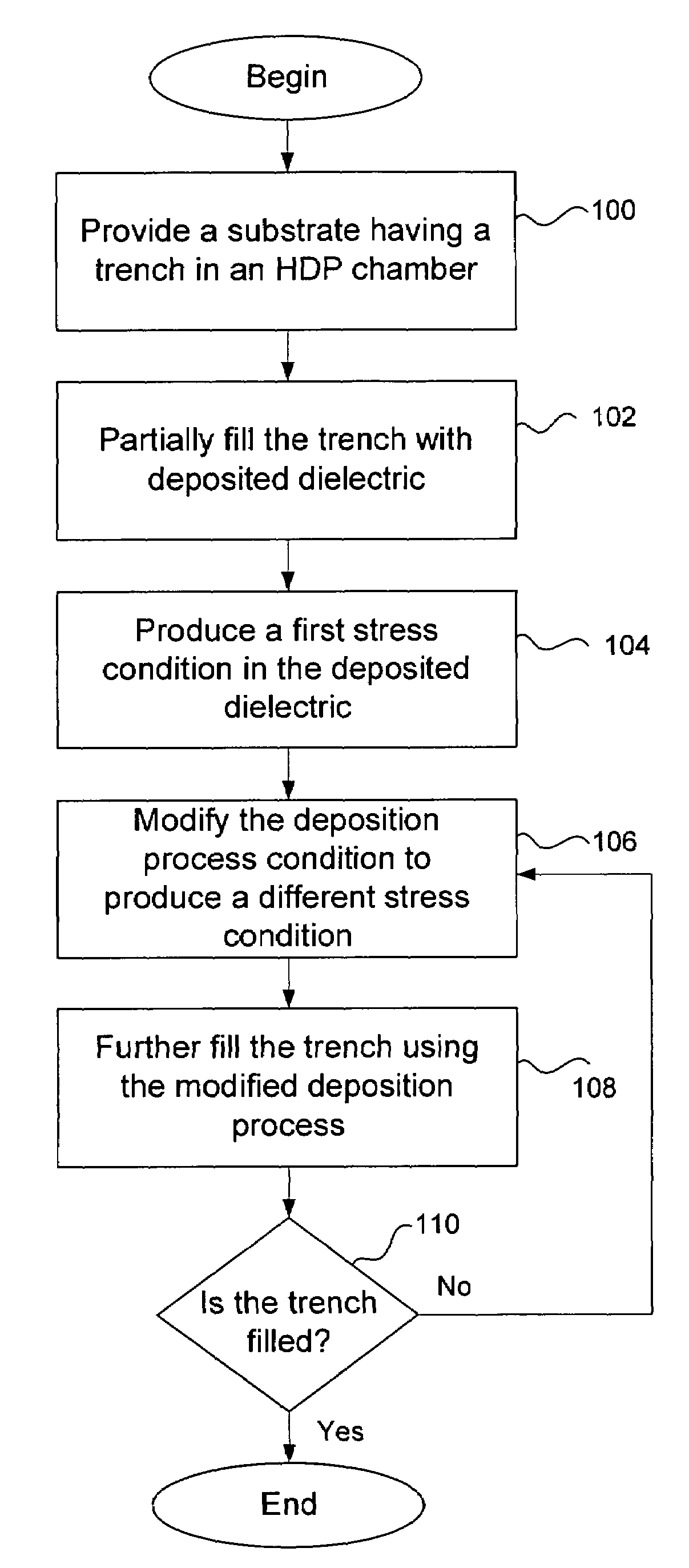
High density plasma (HDP) techniques form silicon oxide films having sequentially modulated stress profiles. The HDP techniques use low enough temperatures to deposit silicon oxide films in transistor architectures and fabrication processes effective for generating channel strain without adversely impacting transistor integrity. Methods involve partially filling a trench on a substrate with a portion of deposited dielectric using a high density plasma chemical vapor deposition process. The conditions of the process are configured to produce a first stress condition in the first portion of the deposited dielectric. The deposition process condition may then be modified to produce a different stress condition in deposited dielectric. The partially-filled trench may be further filled using the modified deposition process to produce additional dielectric and can be repeated until the trench is filled. Transistor strain can be generated in NMOS or PMOS devices using stress profile modulation in STI gap fill.
Description
FIELD OF THE INVENTION[0001]This invention relates to high density plasma (HDP) deposition techniques for forming silicon oxide films. The methods can be used to tailor stress in deposited silicon oxide films in transistor architectures to control channel strain.BACKGROUND[0002]As transistors are scaled to smaller dimensions there is a need for higher switching speeds. One solution to increase transistor speed is to strain the silicon in the channel. Adding a small amount of strain to the silicon lattice structure promotes higher electron and hole mobilities, which increase transistor drain current and device performance.[0003]When the lattice is under tensile strain, its physical symmetry is broken, and with it the electronic symmetry. The lowest energy level of the conduction band is split, with two of the six original states dropping to a lower energy level and four rising to a higher energy level. This renders it more difficult for the electrons to be ‘scattered’ between the low...
Claims
Login to View More Application Information
Patent Timeline
 Patent Type & AuthorityPatents(United States)
IPC IPC(8): H01L21/76
CPCH01L21/823807H01L21/823878H01L29/7846H01L29/665H01L29/78
InventorYU, JENGYILANG, CHI-IHUANG, JUDY H.
OwnerNOVELLUS SYSTEMS