
Monolithic array for solid state ultraviolet light emitters

a solid-state ultraviolet light and monolithic array technology, applied in the field of led, can solve the problems of reducing the optical volume of n- and p-cladding layers, measuring less accurate or reliable, etc., and achieve the effects of reducing the effect of undesired effects, adjusting the output of the device, and improving current spreading

Inactive Publication Date: 2009-01-27
LOCKHEED MARTIN CORP
View PDF11 Cites 3 Cited by
  • Summary
  • Abstract
  • Description
  • Claims
  • Application Information

AI Technical Summary

Benefits of technology

This design enhances the accuracy and reliability of UV light transmission by focusing energy within a narrow band, reducing stray emissions and improving current densities, thus minimizing interference from material defects and increasing the efficiency of UV energy output.

Problems solved by technology

In these instances, generalized emissions (such as through the side of the device), could render the measurement less accurate or reliable.
However, having smaller mesas, less than 100 um in diameter, also reduces the optical volume of n- and p-cladding layers, which may be plagued with sub-band-edge luminescent structural and point defects, allowing light to escape the mesa in a shorter optical path length.

Method used


Image

  • Monolithic array for solid state ultraviolet light emitters
  • Monolithic array for solid state ultraviolet light emitters
  • Monolithic array for solid state ultraviolet light emitters

Examples


Embodiment Construction

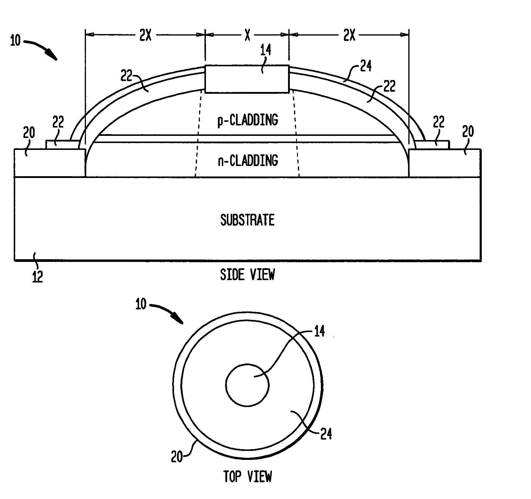
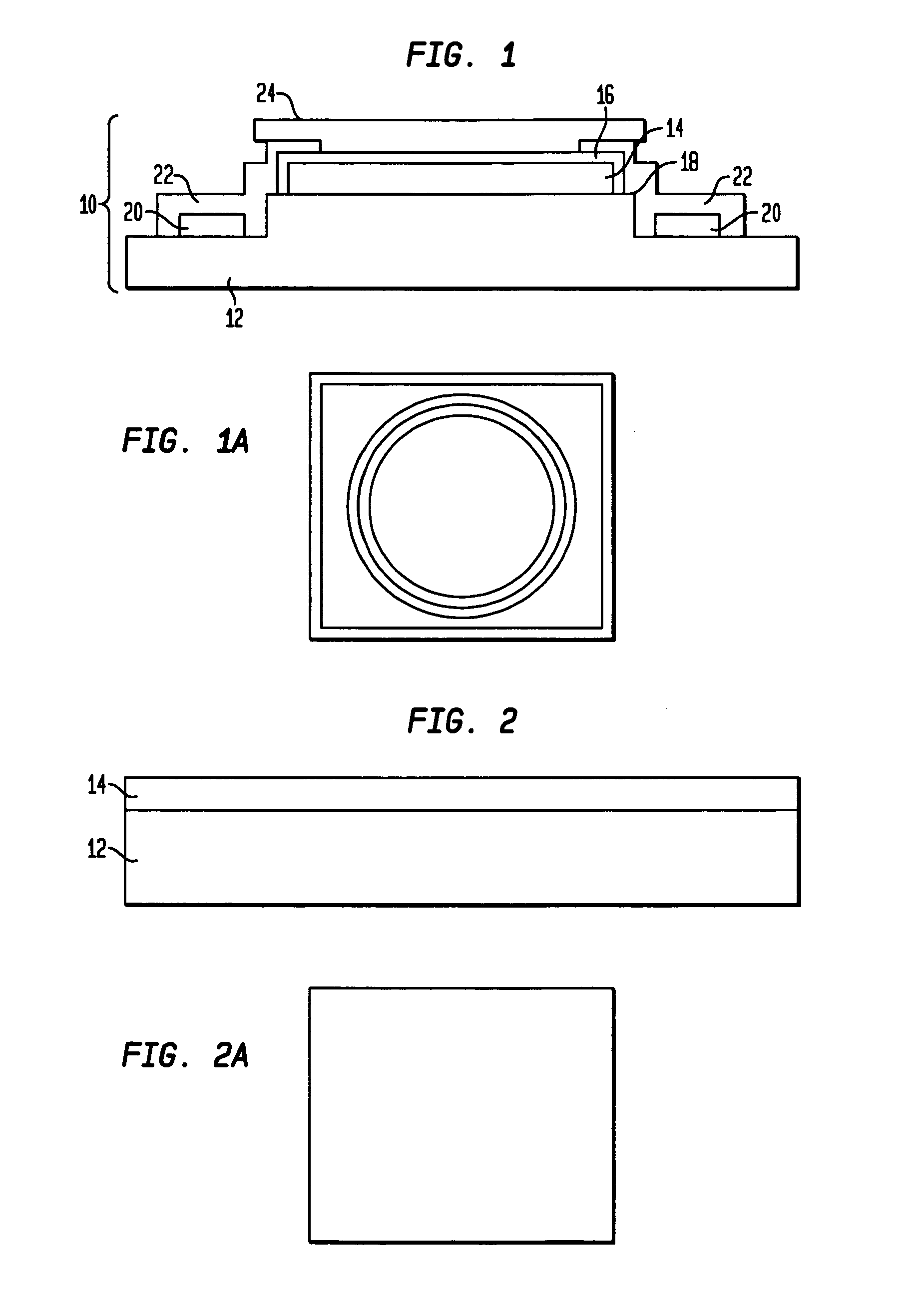
[0043]An LED 10 of the present invention is depicted in FIG. 1. It should be understood that the LED will be incorporated into arrays including a plurality of LED's, which is discussed and shown later in this disclosure.

[0044]LED 10 includes the following components: base layer 12, p-metal layer 14, encapsulant 16, mesa 18, n-metallization layer 20, passivation layer 22, p-bond pad 24 and n-bond pad 26 (not shown in FIG. 1). The bond pads are used to connect the device to a suitable package.

[0045]Base layer 12 is a multiple component element. As depicted in FIG. 8, base layer 12 includes a substrate 30, such as a substrate of sapphire, silicon carbide, zinc oxide, gallium nitride, and any combination of a gallium nitride-aluminum-indium alloy of the formula AlxInyGa1-x-yN, wherein x+y32 is deposited upon the substrate 30. Here the n-doped material may be any conventional material, such as GaN doped with silicon. As shown in FIG. 8, a silicon dopant is present in one or more delta do...


PUM

PropertyMeasurementUnit
diametersaaaaaaaaaa
diametersaaaaaaaaaa
diametersaaaaaaaaaa

Abstract

The present invention is directed towards a source of ultraviolet energy, wherein the source is a UV-emitting LED's. In an embodiment of the invention, the UV-LED's are characterized by a base layer material including a substrate, a p-doped semiconductor material, a multiple quantum well, a n-doped semiconductor material, upon which base material a p-type metal resides and wherein the base structure has a mesa configuration, which mesa configuration may be rounded on a boundary surface, or which may be non-rounded, such as a mesa having an upper boundary surface that is flat. In other words, the p-type metal resides upon a mesa formed out of the base structure materials. In a more specific embodiment, the UV-LED structure includes n-type metallization layer, passivation layers, and bond pads positioned at appropriate locations of the device. In a more specific embodiment, the p-type metal layer is encapsulated in the encapsulating layer.

Description

FIELD OF INVENTION[0001]The present invention is directed to an LED, and arrays of same. In particular, the LED emits energy in the ultra-violet (optical wavelength greater than or equal to 150 nm and less than or equal to 410 nm) portion of the electromagnetic spectrum.BACKGROUND OF THE INVENTION[0002]Consideration has been given to using single color LED's, such as red, blue or green LED's, in combination with fluorescent and phosphorescent materials to produce another desired color. While certain materials respond fluorescently or phosphorescently to light from the visible portion of the spectrum, and thus would respond to visible LED's, there are a number of materials which respond to the relatively higher-energy photons emitted in the ultraviolet portion of the spectrum. Furthermore, UV-emitting LED's may, in combination with the appropriate phosphor, prove to be a source of white light providing a high level of satisfaction. That is, white light generated from a UV LED and acc...

Claims


Application Information

Patent Timeline
Patent Type & Authority Patents(United States)
IPC IPC(8): H01L33/00H01L33/20H01L33/32
CPCH01L27/153H01L33/20H01L33/32
Inventor WOJNAROWSKI, ROBERT JOHNWEAVER, JR., STANTON EARLEBONG, ABASIFREKE UDOCAO, XIAN AN ANDREWLEBOEUF, STEVEN FRANCISROWLAND, LARRY BURTONARTHUR, STEPHEN D.
Owner LOCKHEED MARTIN CORP
Features
  • Generate Ideas
  • Intellectual Property
  • Life Sciences
  • Materials
  • Tech Scout
  • Unparalleled Data Quality
  • Higher Quality Content
  • 60% Fewer Hallucinations
Learn More