Light emitting device, driving method thereof, and image forming apparatus

a technology of light emitting device and driving method, which is applied in the direction of digitally marking record carriers, digital computer details, instruments, etc., can solve the problems of counterbalance of temperature measurement unit errors and difficulty in forming a plurality of oled elements in a uniform manner in an actual head unit, so as to achieve accurate observation and further accurately carry out temperature compensation

Active Publication Date: 2009-02-03
ELEMENT CAPITAL COMMERCIAL CO PTE LTD
View PDF8 Cites 12 Cited by
  • Summary
  • Abstract
  • Description
  • Claims
  • Application Information

AI Technical Summary

Benefits of technology

[0011]It is desirable that the signal data for correcting variation of each light emitting element is stored in the memory unit, and the driving signal based on the signal data read therefrom is applied to the holding units. Specifically, the holding unit may be a volatile memory, and the memory unit may be a non-volatile memory. Since the volatile memory can be simply constructed, the light emitting device having a non-volatile memory chip may be composed of a light emitting panel, in which the plurality of light emitting elements and the plurality of holding units are integrated, and the memory unit in this case, the area of the light emitting panel can be reduced. In addition, yield of the light emitting device can be improved since it can be constructed independently from the non-volatile memory chip.
[0037]It is desirable that the memory unit stores signal data, which indicates the magnitude of the driving signal regulated such that luminosity of the plurality of light emitting elements becomes uniform at the plurality of reference temperatures, respectively, for the plurality of light emitting elements, and in a process of generating the setting signal, as the operation process, the setting unit generates the setting signal by interpolating the signal data at the plurality of reference temperatures read from the memory unit according to the difference between the present temperature and the plurality of reference temperatures. In this case, since the setting signal is generated by interpolating the signal data measured in practice, the temperature compensation can be further accurately carried out.

Problems solved by technology

However, it is difficult to form a plurality of OLED elements in a uniform manner in an actual head unit.
In addition, if the temperature data is generated based on the temperature signal generated by the temperature measurement unit, errors of the temperature measurement unit can be counterbalanced.

Method used


Image

  • Light emitting device, driving method thereof, and image forming apparatus
  • Light emitting device, driving method thereof, and image forming apparatus
  • Light emitting device, driving method thereof, and image forming apparatus

Examples


first embodiment

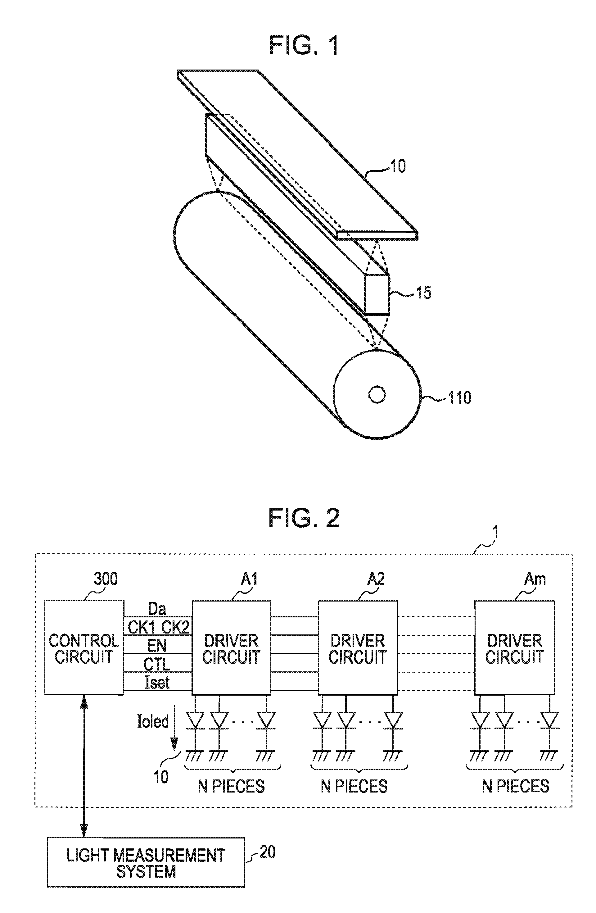
[0064]FIG. 1 is a perspective view showing a portion of an image forming apparatus using a light emitting device according to a first embodiment of the invention. Referring to FIG. 1, the image forming apparatus includes a light emitting device 1, a light condense lens array 15, and a photosensitive drum 110. The light emitting device 1 includes a plurality of light emitting elements disposed in a single line or in multiple lines in an array form. These light emitting elements emit light in a selective manner according to an image to be printed on a recording medium such as a sheet of paper. For example, an organic light emitting diode element (hereinafter referred to as an OLED element) is used as a light emitting element. The light condense lens array 15 is disposed between the light emitting device 1 and the photosensitive drum 110. The light condense lens array 15 includes a plurality of gradient index lenses which are arranged in an array form, while each optical axis thereof f...

second embodiment

[0087]Now, a light emitting device 2 according to a second embodiment of the invention will be described.

[0088]FIG. 13 is a plan view of a light emitting panel 400 used in the light emitting device 2. The driver circuits A1 to Am are omitted in FIG. 13. Referring to FIG. 13, in the light emitting panel 400, OLED elements 10 are formed on a light emission area AA, and optical sensors (measurement units) 31 and 32 are formed at both ends of the light emitting panel 400. The optical sensors 31 and 32 output a measurement signal depending on light quantity of incident light. In this embodiment, the optical sensors 31 and 32 are composed of photodiodes, and output a current depending on light quantity (light intensity) as a measurement signal.

[0089]FIG. 14 is a block diagram of the light emitting device 2. The light emitting device 2 has the same structure as the light emitting device 1 of the first embodiment of FIG. 2, except that a control circuit 301 is used instead of the control ci...

third embodiment

[0096]Hereinafter, an embodiment of a light emitting device suitable for correcting a temperature characteristic (relationship between temperature and light emission brightness) will be described.

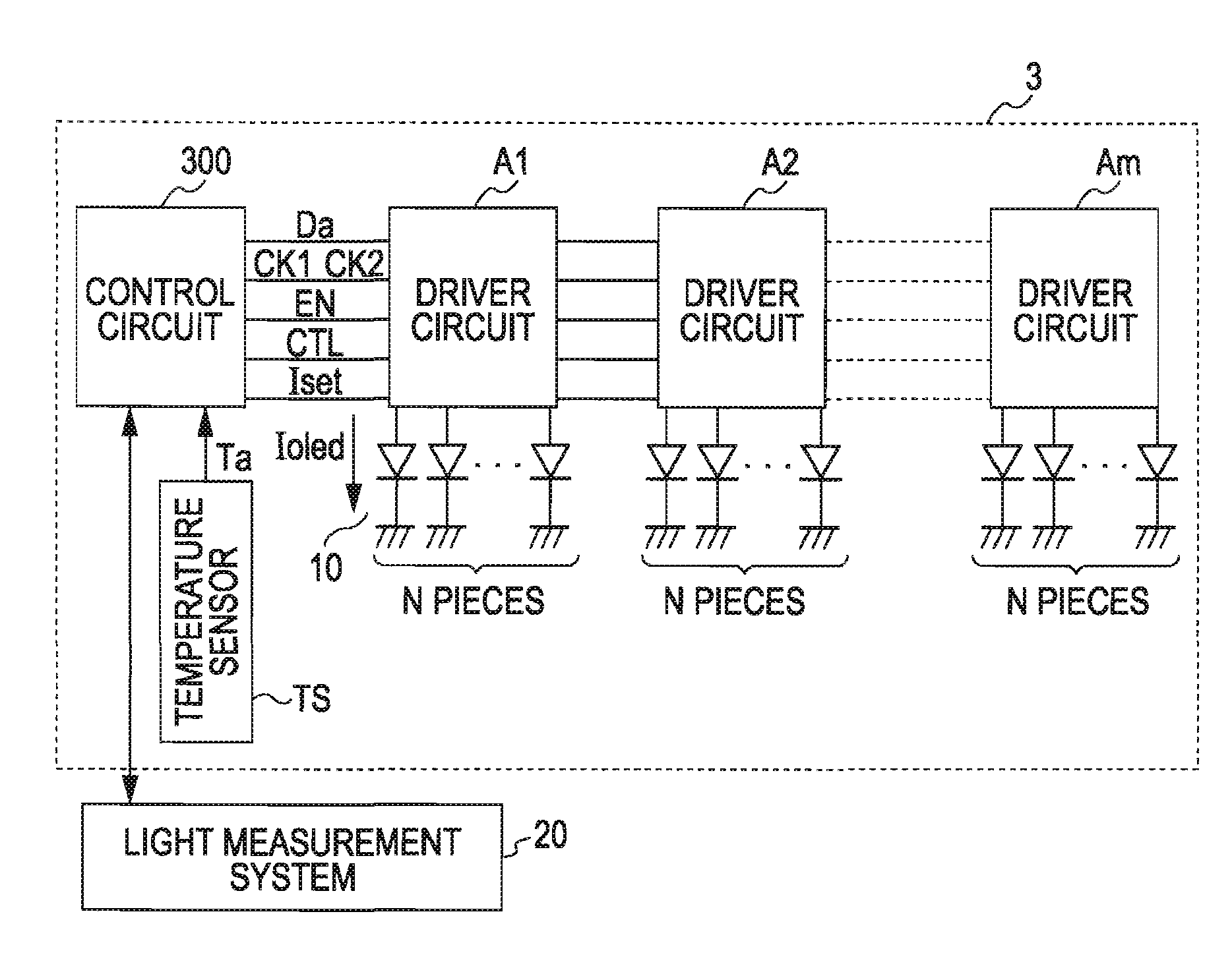
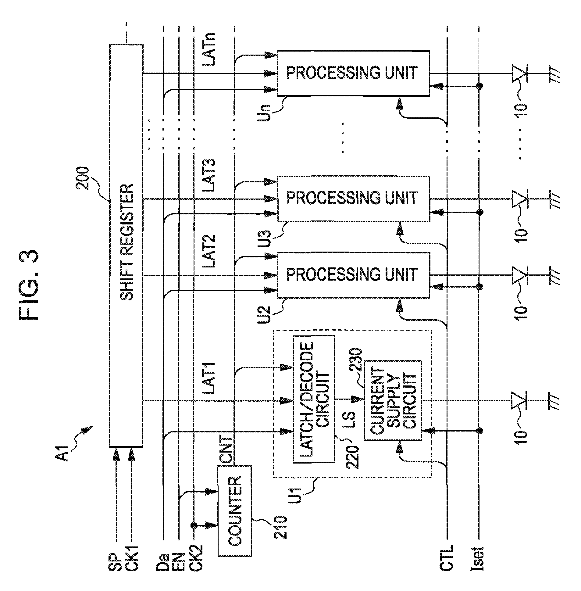
[0097]FIG. 17 is a block diagram of a structure of a light emitting device 3 and a peripheral structure thereof. Referring to FIG. 17, the light emitting device 3 includes m driver circuits A1 to Am, the control circuit 300 controlling the driver circuits A1 to Am, and a temperature sensor (a temperature measurement unit) TS. The temperature sensor TS is closely disposed to the OLED elements 10, and supplies a temperature signal Ta indicating temperature to the control circuit 300. The driver circuits A1 to Am and the control circuit 300 are the same as those in the first embodiment. Thus, each of the driver circuits A1 to Am has the structure of FIG. 3, and each processing unit U1 to Un of the driver circuits A1 to Am has the latch / decode circuit 220, and the aforementioned current control...


PUM


Abstract

A light emitting device includes: a plurality of light emitting elements that emit light to have luminosity depending on the magnitude of a driving signal; a plurality of holding units that are respectively disposed in the plurality of light emitting elements, and respectively hold the driving signal to maintain a magnitude regulated such that the luminosity of the plurality of light emitting elements becomes uniform; and a plurality of supply units that are respectively disposed in the plurality of light emitting elements, and supply the driving signal, which is held by the holding units to have a certain magnitude for a period of time according to a gradation of light to be emitted, to a corresponding light emitting element.

Description

BACKGROUND[0001]1. Technical Field[0002]The present invention relates to a light emitting device using a light emitting material such as an organic EL (Electroluminescent) material, a driving method thereof, and an image forming apparatus using the light emitting device.[0003]2. Related Art[0004]A printer as an image forming apparatus uses a light emitting device in which a plurality of light emitting elements are arranged in an array form as a head unit that forms an electrostatic latent image on an image carrier such as a photosensitive drum or the like. The head unit is generally constructed with a plurality of light emitting elements disposed in a single line along a main scanning direction.[0005]A well-known light emitting element is an organic light emitting diode (hereinafter referred as OLED). In the light emitting element such as an OLED element, light emission intensity in particular, luminosity, changes according to the magnitude of a driving current. As a method of drivi...

Claims


Application Information

Patent Timeline
Patent Type & Authority Patents(United States)
IPC IPC(8): G09G3/36
CPCH04N1/40031H04N1/4015G09G3/30G09G3/20G09G3/32H05B33/02
Inventor NAKAJIMA, AKIRA
Owner ELEMENT CAPITAL COMMERCIAL CO PTE LTD
Why Eureka
Try Eureka