Output power control of an RF amplifier

a technology of output power and amplifier, which is applied in the direction of amplifier, amplification control, electric apparatus, etc., can solve the problems of increased insertion loss along the transmit channel, increased device cost, and limited accuracy of power control, so as to improve precision and reliability, the effect of high efficiency

Inactive Publication Date: 2009-02-10
ST ERICSSON SA
View PDF9 Cites 28 Cited by
  • Summary
  • Abstract
  • Description
  • Claims
  • Application Information

AI Technical Summary

Benefits of technology

[0015]In view of the foregoing background, an object of the present invention is to significantly enhance the precision and reliability of controlling a broad dynamic power range of a high efficiency power amplifier functioning with a non-continuous conduction.
[0017]This advantageously provides precision and robustness of the control by effectively compensating for the fabrication process spread of current gain figures of bipolar junction transistors. Moreover, by employing a band-gap temperature compensation control current that is eventually β-scaled before comparing it with the sensed base current of the output power transistor, the output power may be effectively controlled and maintained constant over temperature as well as process spread variations.

Problems solved by technology

At low power levels, when Vcc approaches VCESAT, accuracy of the power control is limited due to the inability to compensate VCESAT and non-linear effects of temperature variations.
In this case, a directional coupler and power detectors can be used to close the feedback loop with the drawbacks of an increased insertion loss along the transmit channel and a cost increase of the device because of the additional silicon area required.
Therefore, mismatches will occur between the collector currents of the power and of the sense transistor due to a high harmonic content of collector voltage and current waveforms.
These mismatches limit the field of application of the circuit arrangement proposed in [4] to linear power amplifiers or to saturated amplifiers to a limited range of accuracy.

Method used


Image

  • Output power control of an RF amplifier
  • Output power control of an RF amplifier
  • Output power control of an RF amplifier

Examples


Embodiment Construction

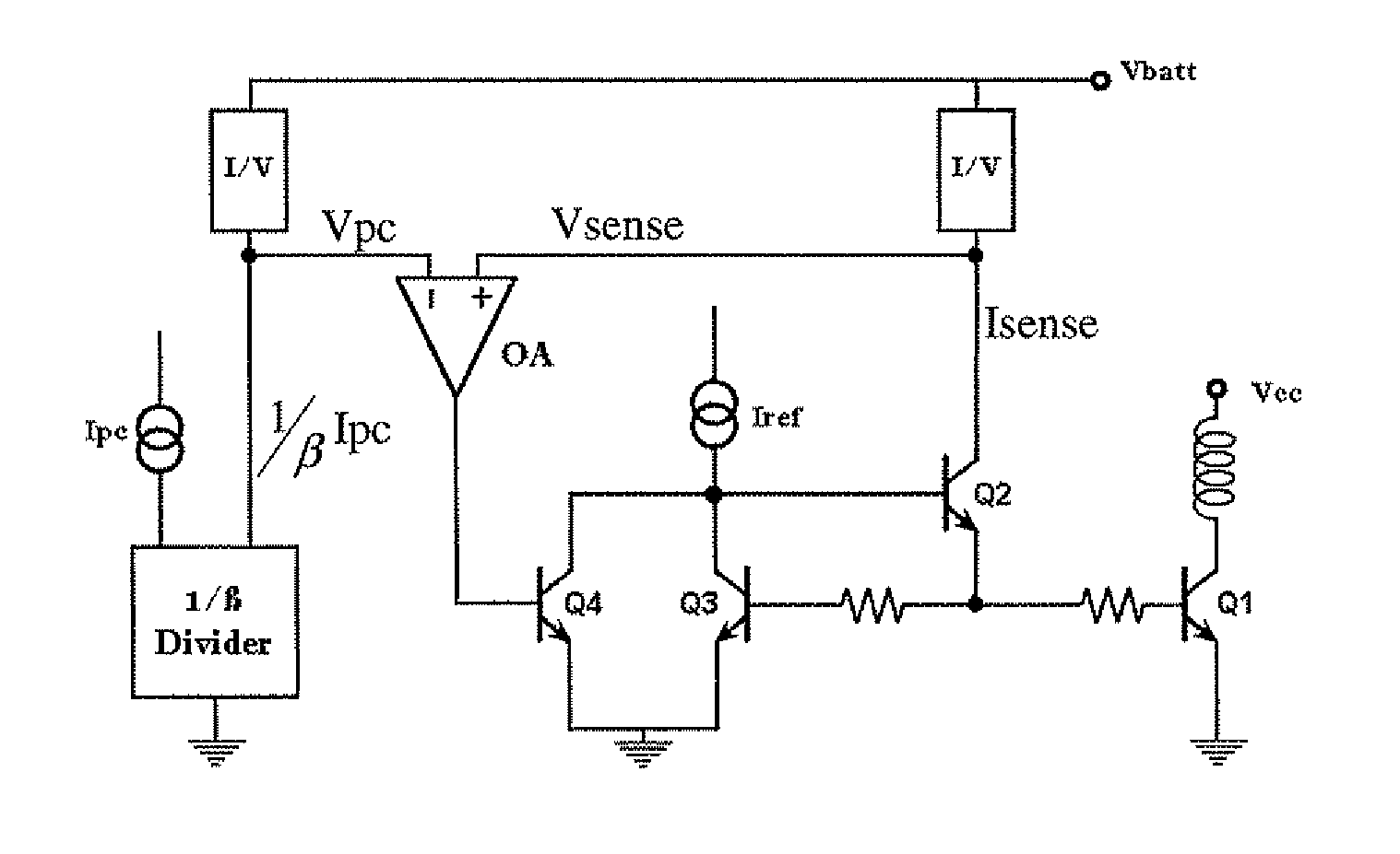
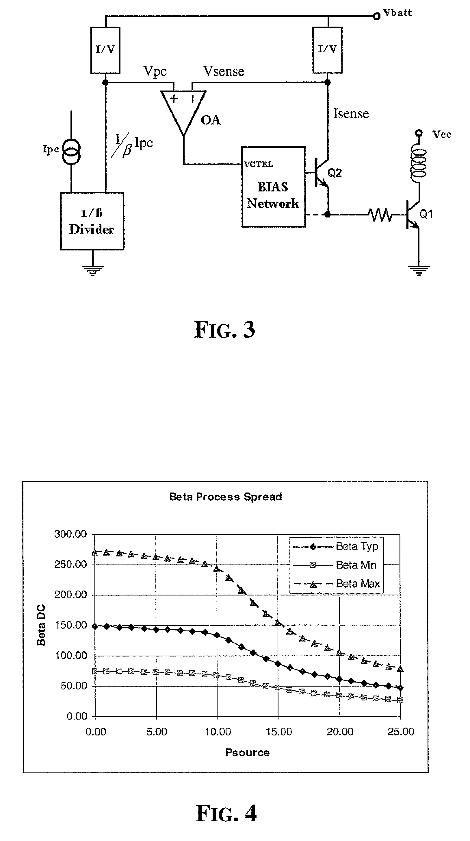
[0031]A basic diagram of the power control bias circuit in accordance with the invention is shown in FIG. 3. According to a fundamental aspect, the base current of the power bipolar transistor Q1 is sensed by an emitter follower sense transistor Q2.

[0032]The base current sensed by transistor Q2 is converted by an I / V block and the resulting voltage signal Vsense is compared by the error amplifier OA with a power control signal Vpc. The power control signal Vpc is produced by similarly converting a β-scaled control current 1 / β Ipc. A control current generator generates a current Ipc that is then divided by the circuit block 1 / β Divider by the current gain (β) of a bipolar junction transistor of the same type of the output transistor Q1 to produce a β-scaled control circuit 1 / β Ipc. The error signal, output by the error amplifier OA, drives the input control signal Vctrl of a biasing network.

[0033]Depending on the arrangement of the biasing network, the negative feedback loop that clo...


PUM


Abstract

Precision and reliability of a current limited mode output power control of an RF amplifier is enhanced by sensing the base current of the current controlled output power transistor. The base current is compared to a control current that is normalized by scaling it as a function of the current gain of a bipolar junction transistor of similar characteristics as the output power transistor. Fabrication process spread of current gain figures of bipolar junction transistors is effectively compensated. Moreover, by using a band-gap temperature compensation control current that is eventually β-scaled before comparing it with the sensed base current of the output power transistor, the output power may be effectively controlled and maintained constant over temperature as well as process spread variations.

Description

FIELD OF THE INVENTION[0001]The present invention relates to sensing and control of an output power signal from an electronic amplifier, and in particular, a radio frequency (RF) power amplifier.BACKGROUND OF THE INVENTION[0002]The demand for power amplifiers for wireless handsets is growing at a rapid rate. Communication standards such as GSM, EDGE and DCS require precise output power control of the power amplifier (PA). Generally, a current controlled bipolar transistor is used, such as a BJT or an HBT, to improve signal to noise ratio of receiver channels. At the same time, talk time and battery life are increased by reducing power consumption of the transmitter.[0003]Moreover, overall system efficiency of a GSM / EDGE transmitter can be increased using polar architectures [1]. In this case, bias circuits to control the PA output power, with large dynamic range and no degradation on efficiency and linearity, need to be designed to comply with system specifications.[0004]A voltage l...

Claims


Application Information

Patent Timeline
Patent Type & Authority Patents(United States)
IPC IPC(8): H03G3/30
CPCH03F1/0261H03F1/302H03F2200/18H03F2200/447H03F2200/456H03F2200/462H03F2200/78
Inventor VAIANA, MICHELEGRAMEGNA, GIUSEPPE
Owner ST ERICSSON SA
Why Eureka
Try Eureka