Buffer circuit having multiplexed voltage level translation

a buffer circuit and voltage level technology, applied in electronic switching, pulse automatic control, pulse technique, etc., can solve the problem of large chip area, achieve the effect of reducing chip area, enhancing buffer circuit, and reducing the overall size of the integrated circui

Active Publication Date: 2009-03-03
GENERAL ELECTRIC CO +1
View PDF2 Cites 13 Cited by
  • Summary
  • Abstract
  • Description
  • Claims
  • Application Information

AI Technical Summary

Benefits of technology

[0005]The present invention meets the above-noted need by providing, in an illustrative embodiment thereof, an enhanced buffer circuit having reduced chip area compared to standard buffer circuits. To accomplish this, an embodiment of the invention utilizes multiplexing of two or more control signals supplied to the buffer circuit so as to share a single voltage level translator circuit, thereby utilizing a fewer number of voltage level translator circuits and reducing the overall size of the integrated circuit.

Problems solved by technology

Unfortunately, however, each voltage level translator circuit consumes a significant amount of chip area in an integrated circuit device, and therefore the number of voltage level translator circuits in the integrated circuit should be minimized.

Method used


Image

  • Buffer circuit having multiplexed voltage level translation
  • Buffer circuit having multiplexed voltage level translation
  • Buffer circuit having multiplexed voltage level translation

Examples


Embodiment Construction

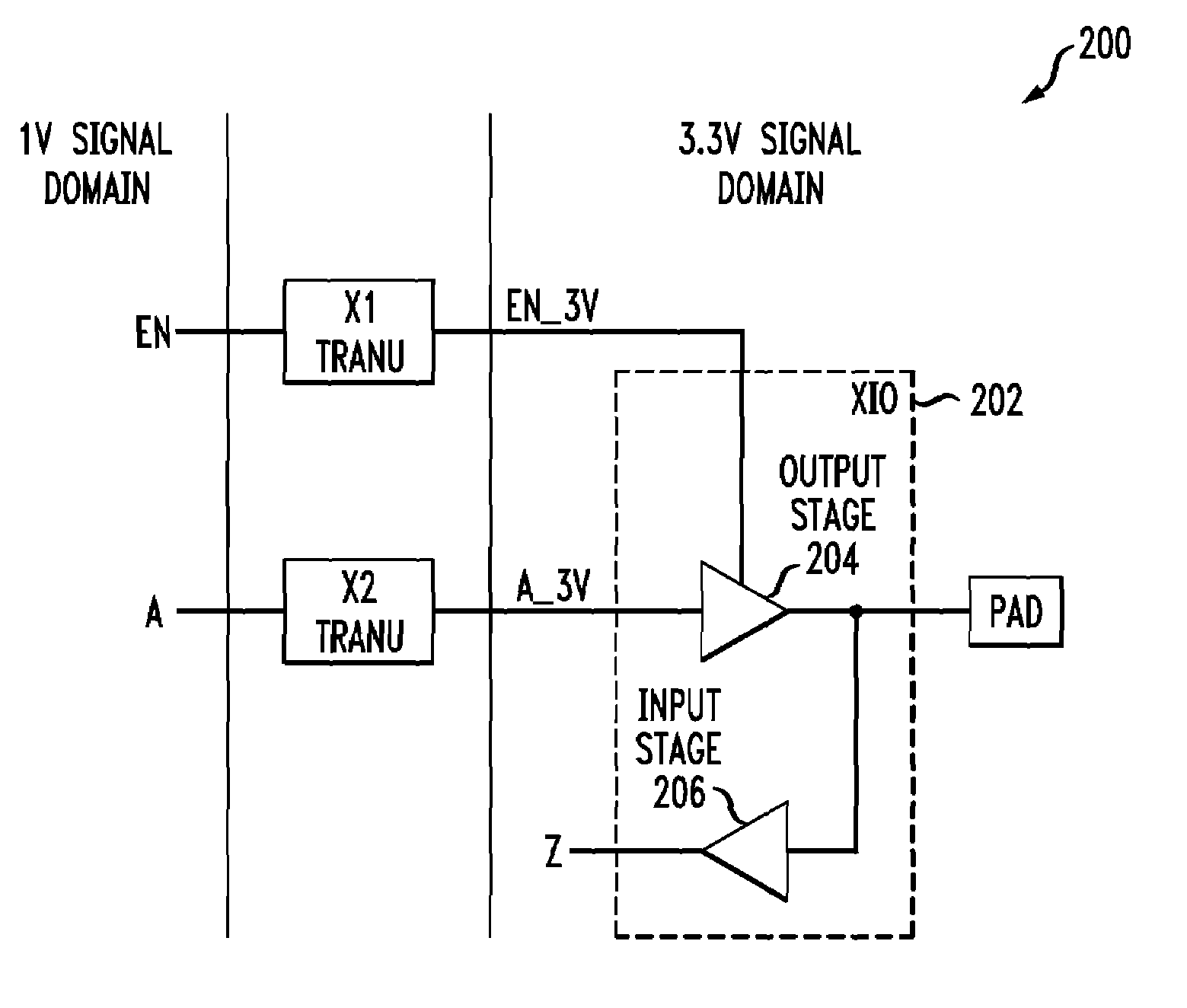
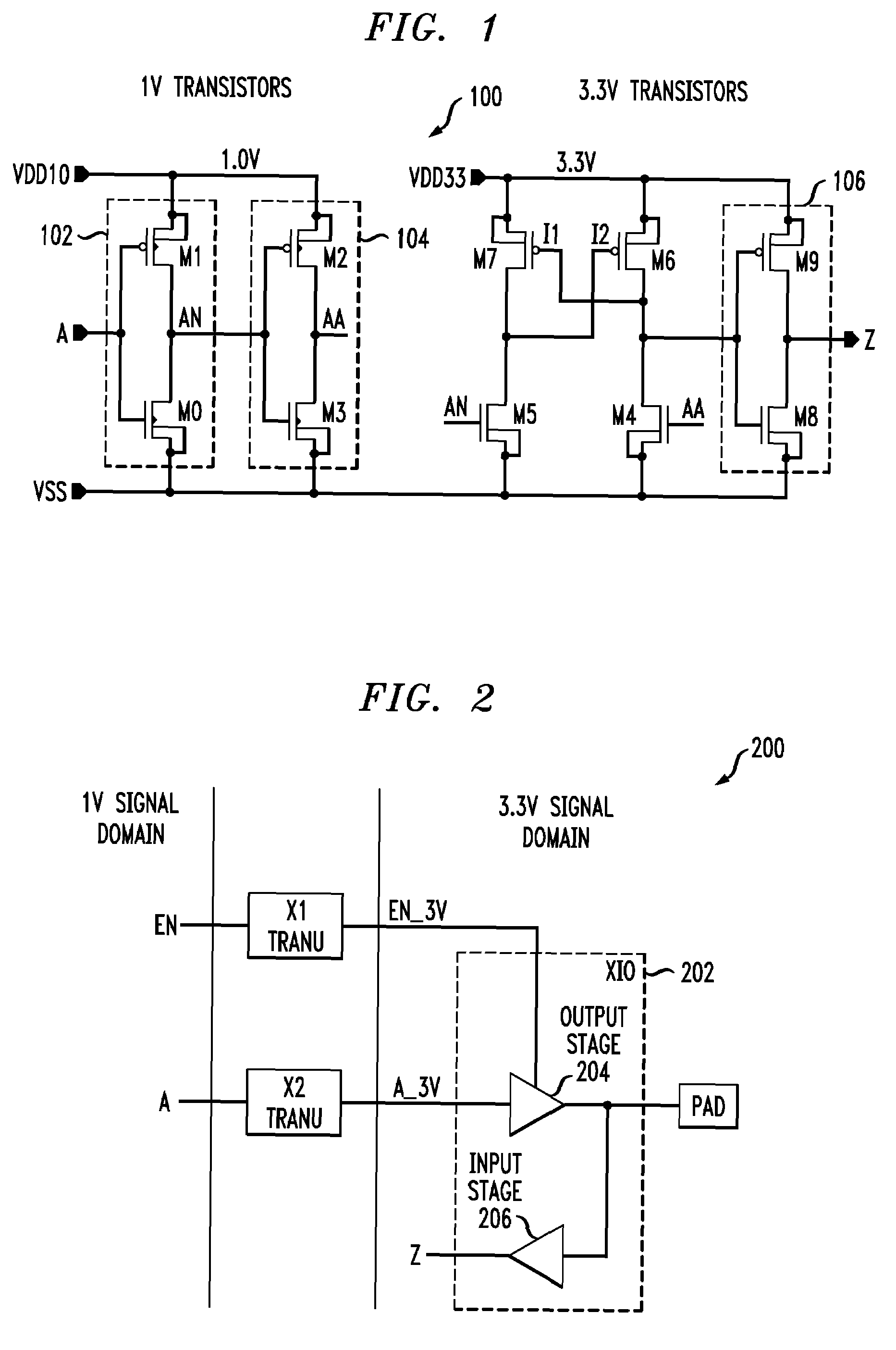
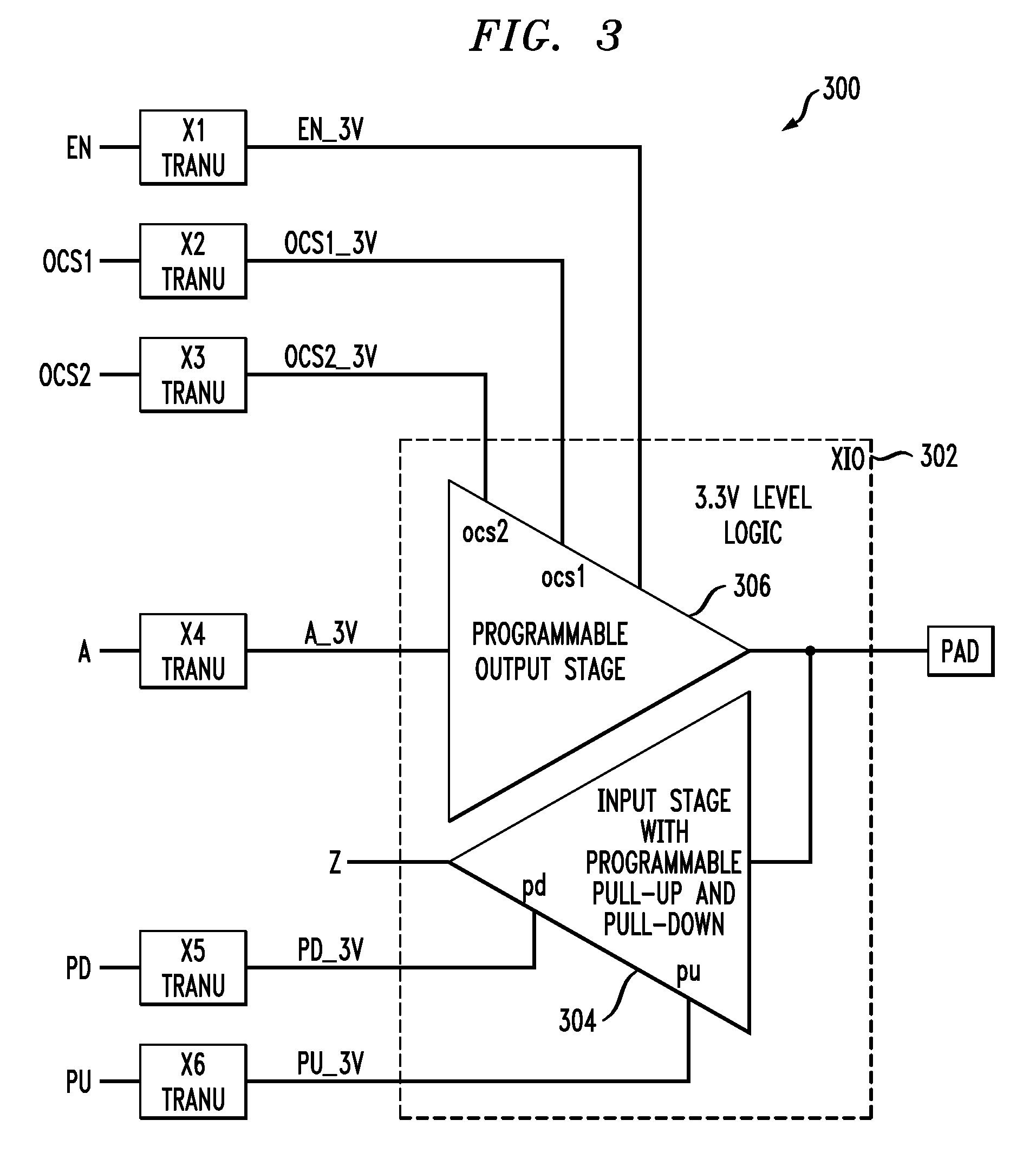
[0015]The present invention will be described herein in the context of illustrative voltage level translator and bidirectional buffer circuits. It should be understood, however, that the present invention is not limited to these or any other particular circuit arrangements. Rather, the invention is more generally applicable to techniques for reducing the chip area of a bidirectional buffer circuit. To accomplish this, embodiments of the invention utilize a multiplexing arrangement whereby two or more control signals supplied to the bidirectional buffer circuit share a single voltage level translator circuit, thereby reducing the number of voltage level translator circuits required by the buffer circuit.

[0016]Although implementations of the present invention are described herein with specific reference to p-channel metal-oxide-semiconductor (PMOS) and n-channel metal-oxide-semiconductor (NMOS) transistor devices, as may be formed using a complementary metal-oxide-semiconductor (CMOS)...


PUM


Abstract

A buffer circuit is selectively operative in one of at least a first mode and a second mode as a function of a first control signal supplied to the buffer circuit. The buffer circuit includes interface circuitry operative to receive at least second and third control signals referenced to a first voltage level, and to generate an output signal referenced to a second voltage level, the second voltage level being greater than the first voltage level. The output signal is a function of the second control signal in the first mode and is a function of the third control signal in the second mode. The buffer circuit further includes at least first and second circuit portions coupled to the interface circuitry, each of the first and second circuit portions including at least one control input operative to receive the output signal generated by the interface circuitry.

Description

FIELD OF THE INVENTION[0001]The present invention relates generally to electronic circuits, and more particularly relates to bidirectional buffer circuits.BACKGROUND OF THE INVENTION[0002]Certain portable devices, including wireless handsets, notebook computers and personal digital assistants (PDAs), often employ circuitry which runs on two or more different voltage levels. For instance, circuitry utilized with such portable devices may be configured so that a portion of the circuitry, such as, for example, input / output (IO) buffers, runs at a higher voltage level (e.g., about 3.3 volts), as may be supplied by an IO voltage source, while another portion of the circuitry, such as, for example, core logic, runs at a substantially lower voltage level (e.g., about 1.0 volt), as may be supplied by a core voltage source. This difference in voltage levels often necessitates the use of a voltage level translator circuit for interfacing between the multiple voltage levels.[0003]There are man...

Claims


Application Information

Patent Timeline
Patent Type & Authority Patents(United States)
IPC IPC(8): H03L5/00
CPCH03K19/017581H03K19/01759
Inventor BHATTACHARYA, DIPANKARHUBER, CAROL A.KOTHANDARAMAN, MAKESHWARKRIZ, JOHN C.MORRIS, BERNARD L.
Owner GENERAL ELECTRIC CO
Why Eureka
Try Eureka