Method of forming polycrystalline semiconductor layer and thin film transistor using the same

a technology of polycrystalline semiconductors and thin film transistors, which is applied in the direction of semiconductor devices, instruments, electrical equipment, etc., can solve the problems of large variation in grain size, high cost of fabricating driving circuits, and large cost of lcd devices using driving circuits, so as to achieve uniform grain size and uniform distance

Active Publication Date: 2009-03-24
LG DISPLAY CO LTD
View PDF5 Cites 19 Cited by
  • Summary
  • Abstract
  • Description
  • Claims
  • Application Information

AI Technical Summary

Benefits of technology

[0019]An object of the present invention is to provide a method of forming a polycrystalline silicon layer having uniform grain size and uniform distance between adjacent grains.

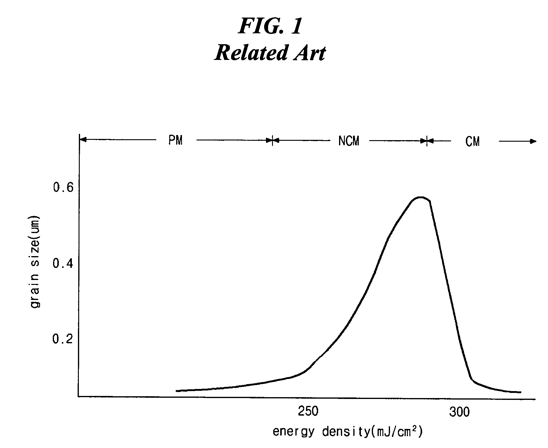
Problems solved by technology

However, since the costs of fabricating the driving circuits are relatively high, costs of LCD devices using the driving circuits is also relatively high.
However, within the NCM regime, grain size variation is large due to an energy density of the laser beam.
Thus, since grain size greatly varies even with small changes of the energy density, the ELA process has a narrow process window for achieving optimum results, wherein the process window is a process error margin where deterioration does not occur.
As the process window becomes narrower, production yield decreases and production costs increase.
For example, when an energy density of 260 mJ / cm2 is set for the laser beam, the excimer laser cannot irradiate a laser beam having an exact energy density of 260 mJ / cm2 due to an inherent error of the excimer laser apparatus.
Accordingly, grain size and distances between the grains are not uniform in the layer of polycrystalline silicon.
Thus, the non-uniformity of the grain sizes deteriorates operational characteristics of a TFT using the polycrystalline layer 13.

Method used


Image

  • Method of forming polycrystalline semiconductor layer and thin film transistor using the same
  • Method of forming polycrystalline semiconductor layer and thin film transistor using the same
  • Method of forming polycrystalline semiconductor layer and thin film transistor using the same

Examples


Embodiment Construction

[0034]Reference will now be made in detail to the preferred embodiments of the present invention, examples of which are illustrated in the accompanying drawings.

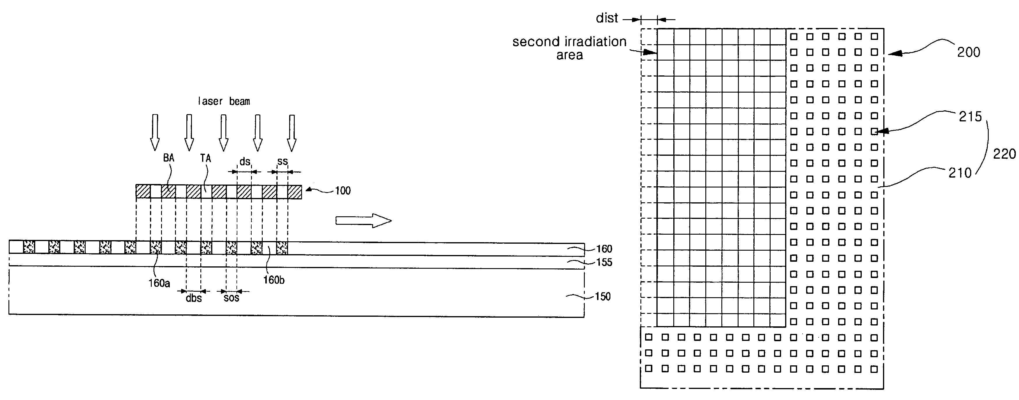
[0035]FIG. 3A is a schematic plan view of an exemplary crystallization mask according to the present invention, and FIG. 3B is an enlarged view of a portion “A” of FIG. 3A according to the present invention. In FIGS. 3A and 3B, a crystallization mask 100 may have a rectangular shape, wherein a width WM and a length LM of the crystallization mask 100 may be determined by laser beam characteristics of an excimer laser apparatus. For example, the laser beam used in an excimer laser annealing (ELA) method may have a width of about 0.1 mm to about 0.3 mm and a length of about several tens of millimeters to about several hundreds of millimeters. Thus, the crystallization mask 100 may have a width greater than a width of the laser beam and a length greater than a length of the laser beam to shield the laser beam entirely.

[0036]In a...


PUM

PropertyMeasurementUnit
distanceaaaaaaaaaa
widthaaaaaaaaaa
distances ds1aaaaaaaaaa

Abstract

A method of forming a polycrystalline semiconductor layer includes forming a semiconductor layer of amorphous silicon on a substrate, forming a plurality of spot seeds in the semiconductor layer by irradiating a first laser beam through a crystallization mask, each of the plurality of spot seeds being equally spaced from one another and each having equal area, and forming a polycrystalline silicon layer along an entire surface of the substrate by irradiating a second laser beam onto the semiconductor layer.

Description

[0001]The present invention claims the benefit of Korean Patent Application No. 2003-0064455, filed in Korea on Sep. 17, 2003, which is hereby incorporated by reference.BACKGROUND OF THE INVENTION[0002]1. Field of the Invention[0003]The present invention relates to a method of forming a semiconductor layer, and more particularly, to a method of crystallizing amorphous silicon for a flat panel display device and a thin film transistor fabricated using a method of crystallizing amorphous silicon.[0004]2. Discussion of the Related Art[0005]Presently, flat panel display (FPD) devices are being developed having high portability and low power consumption. Among various types of FPD devices, liquid crystal display (LCD) devices are commonly used as monitors for notebook and desktop computers because of their ability to display high resolution images, wide ranges of different colors, and moving images.[0006]In general, an LCD device includes a color filter substrate and an array substrate s...

Claims


Application Information

Patent Timeline
Patent Type & Authority Patents(United States)
IPC IPC(8): H01L21/76G02F1/13H01L21/20H01L21/336H01L21/77H01L21/84H01L27/12H01L29/786
CPCH01L21/2026H01L29/66757H01L29/78675H01L27/1285H01L21/02686H01L21/02678H01L21/02488H01L21/02422H01L21/02532H01L21/02691G02F1/13H01L21/02595H01L21/0268
Inventor YOU, JAESUNG
Owner LG DISPLAY CO LTD
Why Eureka
Try Eureka