
Method for applying rewiring to a panel while compensating for position errors of semiconductor chips in component positions of the panel

a technology of semiconductor chips and component positions, applied in electrical testing, instruments, electrical apparatus, etc., can solve the problems of time-consuming method, chip position inaccuracy, and large failure of yield, so as to reduce rejects, shorten process duration, and improve alignment. the effect of accuracy

Inactive Publication Date: 2009-04-07
POLARIS INNOVATIONS LTD
View PDF10 Cites 14 Cited by
  • Summary
  • Abstract
  • Description
  • Claims
  • Application Information

AI Technical Summary

Benefits of technology

"The invention provides a method for applying rewiring to a panel while compensating for position errors of semiconductor chips in the component positions of the panel. The method uses two masks, one for external contact areas and one for rewiring lines. The first mask is used to prepare external contact areas for the panel, while the second mask is used to transfer the rewiring pattern. The second mask compensates for position errors of the semiconductor chips in the individual component positions of the panel. The method allows for improved compensation for position inaccuracies of the semiconductor chips, reduces the size of the contact areas, and increases the rewiring density. The use of optical position registration and evaluation of position errors of the semiconductor chips in the panel optimizes the alignment of the overall rewiring mask during the first exposure."

Problems solved by technology

However, within the panel, the problem arises that the chips to be wired exhibit position inaccuracies because of the population tolerances during the production of the panel.
Position inaccuracies of this type can lead to considerable failures in the yield occurring with the conventional exposure processes of photolithography.
However, because of the high rewiring densities required on a panel and the size of the area to be exposed for each panel, this exposure by means of scanning with a laser write beam is a time-consuming method and disadvantageously associated with high process costs.
This method likewise results in a low throughput as a result of the sequential processing of the panel, as compared to the use of a single overall mask which manages with one exposure process.
A further disadvantage is that, as a result of the independent adjustment of each individual installation location, although the position errors of the semiconductor chips are compensated for, the individual alignment means that a uniform grid no longer results for the matrix and the pattern of the external contacts.
Such a nonuniform pattern of the external contact areas on account of the position errors of the semiconductor chips also leads to problems in applying the external contacts in the form of solder globules in a compliant manner, since both the printing processes and the deposition by electroplating, and the mechanical alignment of solder globules assume a defined and reproducible pattern dimension within the context of a uniform matrix.
This can in turn lead to problems during testing and during the further processing or the use of the electronic components in a fabrication plant if the position errors become greater than those permitted by the JEDEC Standards.
Arranged in the component positions are semiconductor chips whose edges are not aligned accurately in accordance with the rows and columns, which results in position errors.
However, these rewiring lines do not extend as far as the contact areas of the semiconductor chip in the individual component positions, but only approximately as far as the edges of the semiconductor chips.
However, on account of the short writing length of the line pieces which still have to be implemented, the method is more cost-effective than complete production of the rewiring structure of the panel by laser structuring by means of a laser write beam.

Method used


Image

  • Method for applying rewiring to a panel while compensating for position errors of semiconductor chips in component positions of the panel
  • Method for applying rewiring to a panel while compensating for position errors of semiconductor chips in component positions of the panel
  • Method for applying rewiring to a panel while compensating for position errors of semiconductor chips in component positions of the panel

Examples


Embodiment Construction

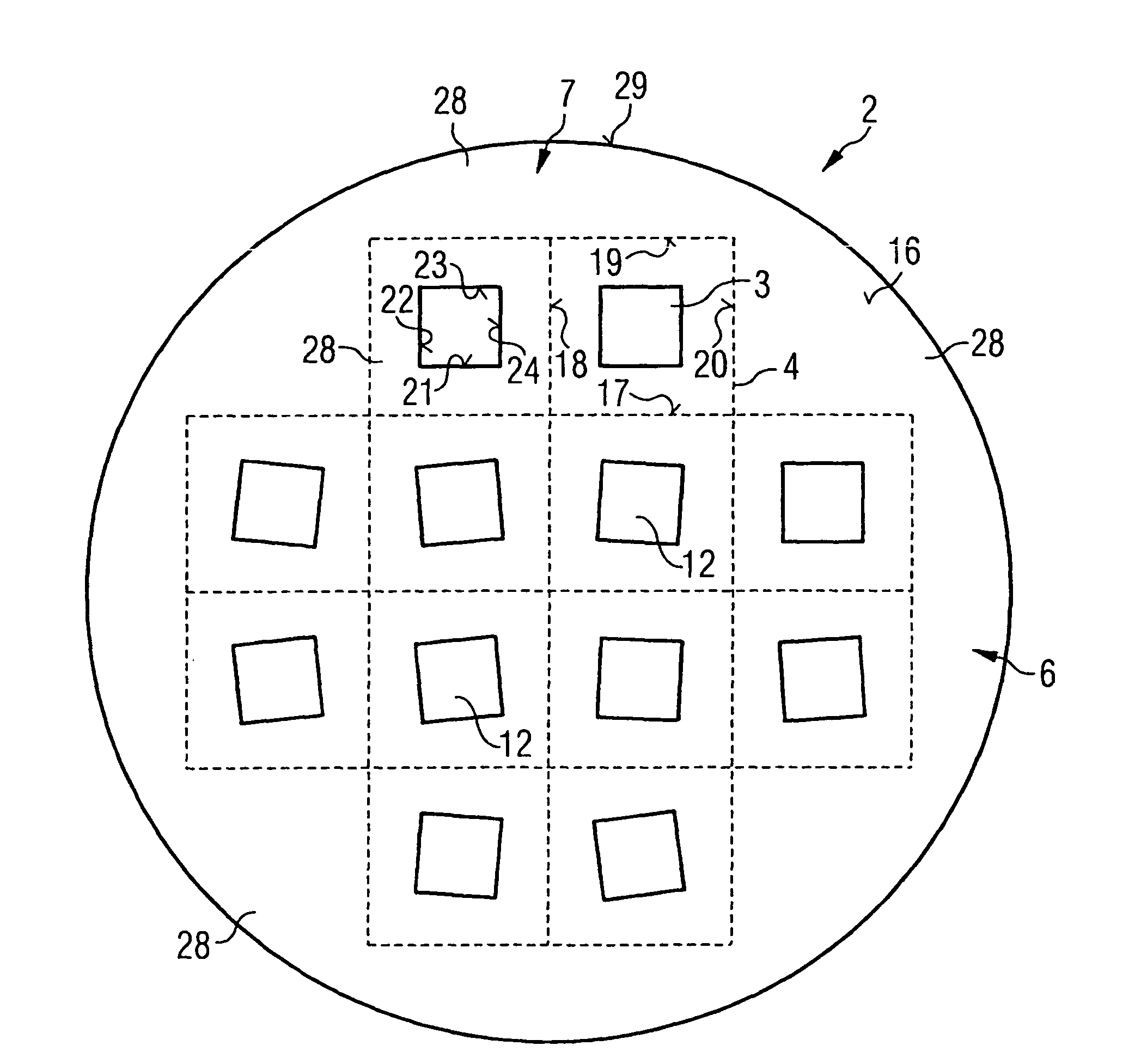
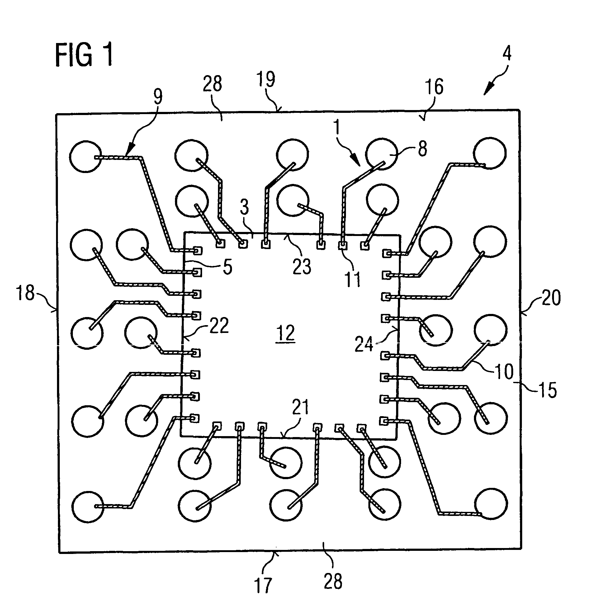
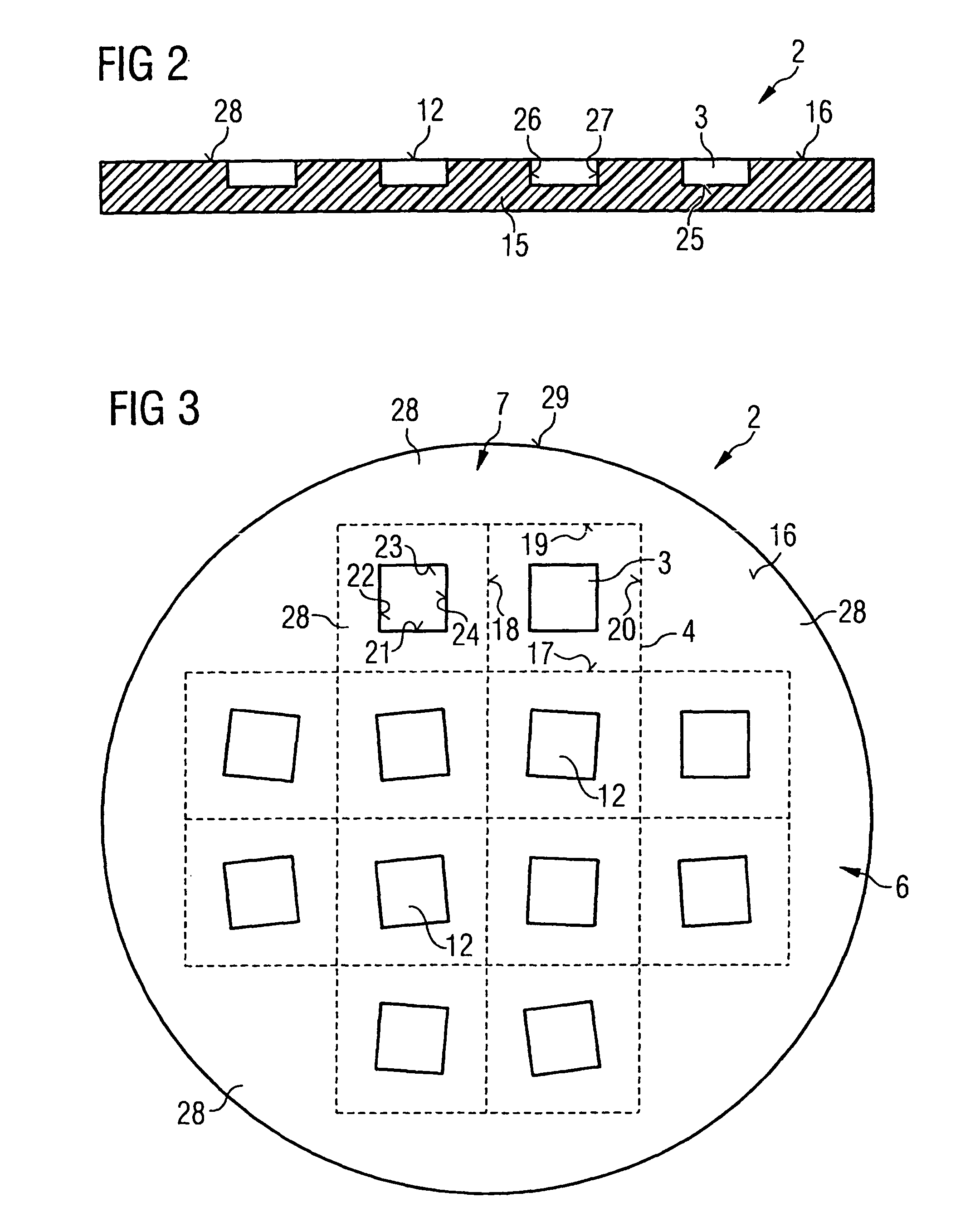
[0029]FIG. 1 illustrates a schematic plan view of a component position 4 of a panel according to a first example of the implementation of the method of the invention. To this end, this plan view shows the overall upper side 16 of such a component position 4. This overall upper side 16 is composed of a coplanar upper side 28 of a plastic compound 15 and an active upper side 12 of a semiconductor chip 3. Rewiring 1 is arranged on the overall upper side 16.

[0030]During the production of a panel which has such a component position 4, the semiconductor chip 3 is embedded in the plastic compound 15 with its rear side and its edge sides, which cannot be seen in this plan view. During this embedding, it is possible for position inaccuracies to occur which, in this plan view, can be seen from the fact that the boundary lines 17, 18, 19 and 20 of the component position 4 do not run parallel to the edges 21, 22, 23 and 24 of the semiconductor chip 3.

[0031]By contrast, the external contact area...


PUM


Abstract

The invention relates to a method for applying rewiring to a panel. For this purpose, a panel is provided which has a coplanar overall upper side of an upper side of a plastic compound and the upper sides of semiconductor chips. The method provides a rewiring layer with implementation of external contacts and rewiring lines which, by means of a two-stage exposure step, compensates for position errors of the semiconductor chips in the component positions of the panel.

Description

CROSS-REFERENCE TO RELATED APPLICATION[0001]This Utility Patent Application claims the benefit of the filing date of application No. DE 103 34 577.9, filed Jul. 28, 2003 and International Application No. PCT / DE2004 / 001360 filed Jun. 28, 2004, both of which are herein incorporated by reference.FIELD OF THE INVENTION[0002]The invention relates to a method for applying rewiring to a panel while compensating for position errors of semiconductor chips in component positions of the panel.BACKGROUND OF THE INVENTION[0003]In applications which are based on embedding a semiconductor chip in a polymer or plastic compound in such a way that the upper sides of semiconductor chip and plastic compound form an overall upper side, such as is provided, for example, in multi-chip module technology or MCM technology or in chip-in-polymer technology, starting from the active upper sides of the semiconductor chips with their contact areas, rewiring is needed in order to connect the contact areas of the ...

Claims


Application Information

Patent Timeline
Patent Type & Authority Patents(United States)
IPC IPC(8): H01L21/20H01L21/60H01L23/538
CPCH01L23/5389H01L24/19H01L24/25H01L22/12H01L22/20H01L2224/04105H01L2224/20H01L2924/01004H01L2924/0101H01L2924/01032H01L2924/01057H01L2924/01079H01L2924/01082H01L2924/12044H01L2924/15173H01L2924/01033H01L2924/01068H01L2924/01084H01L24/96
Inventor HEDLER, HARRYPOHL, JENSWOERNER, HOLGER
Owner POLARIS INNOVATIONS LTD
Learn More