Interleaved memory cell with single-event-upset tolerance

a memory cell and tolerance technology, applied in the field of complementary metaloxidesemiconductor (“ cmos”) memory cells, can solve the problems of significant deformation of latch performance, upset data value stored at a node, and memory cell layout appropriate for a larger technology design dimension (e.g., 90 nm technology) might not provide adequate seu toleran

Active Publication Date: 2009-04-07
XILINX INC
View PDF8 Cites 24 Cited by
  • Summary
  • Abstract
  • Description
  • Claims
  • Application Information

AI Technical Summary

Problems solved by technology

One approach is commonly called “resistive hardening;” however, resistive hardening can significantly degrade latch performance.
Another disadvantage arises if a standard CMOS fabrication has to be modified to accommodate a resistively hardened IC.
This charge can upset the data value stored at a node by changing the voltage at that node.
As the design technology decreases for IC production, a memory cell layout appropriate for a larger technology design dimension (e.g., 90 nm technology) might not provide adequate SEU tolerance when reduced to a smaller design dimension (e.g., 65 nm technology) product.
For example, an SEU tolerant cell layout that provides sufficient spacing between redundant nodes in a 90 nm design might provide insufficient spacing when reduced to a 65 nm design.

Method used


Image

  • Interleaved memory cell with single-event-upset tolerance
  • Interleaved memory cell with single-event-upset tolerance
  • Interleaved memory cell with single-event-upset tolerance

Examples


Embodiment Construction

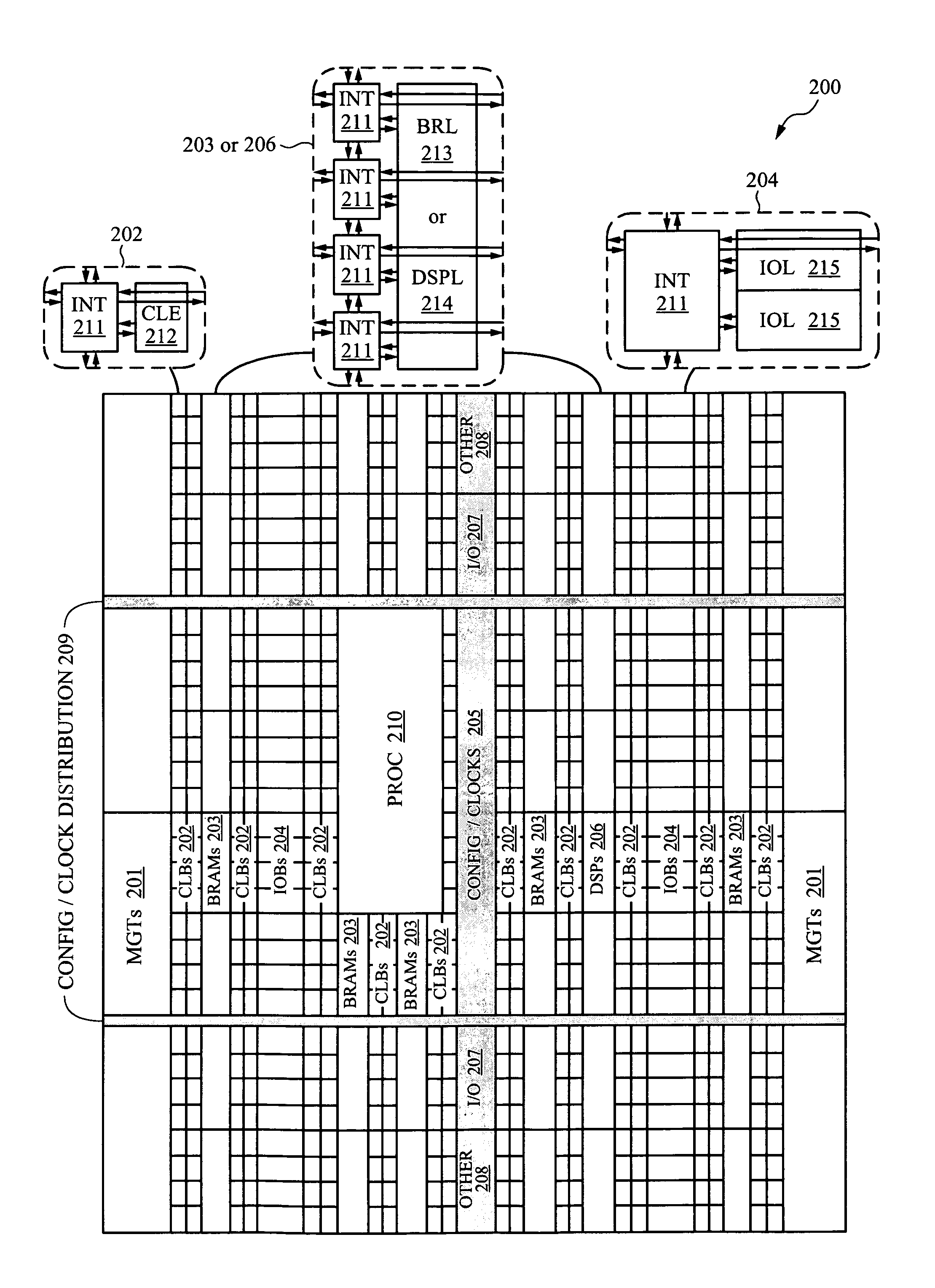
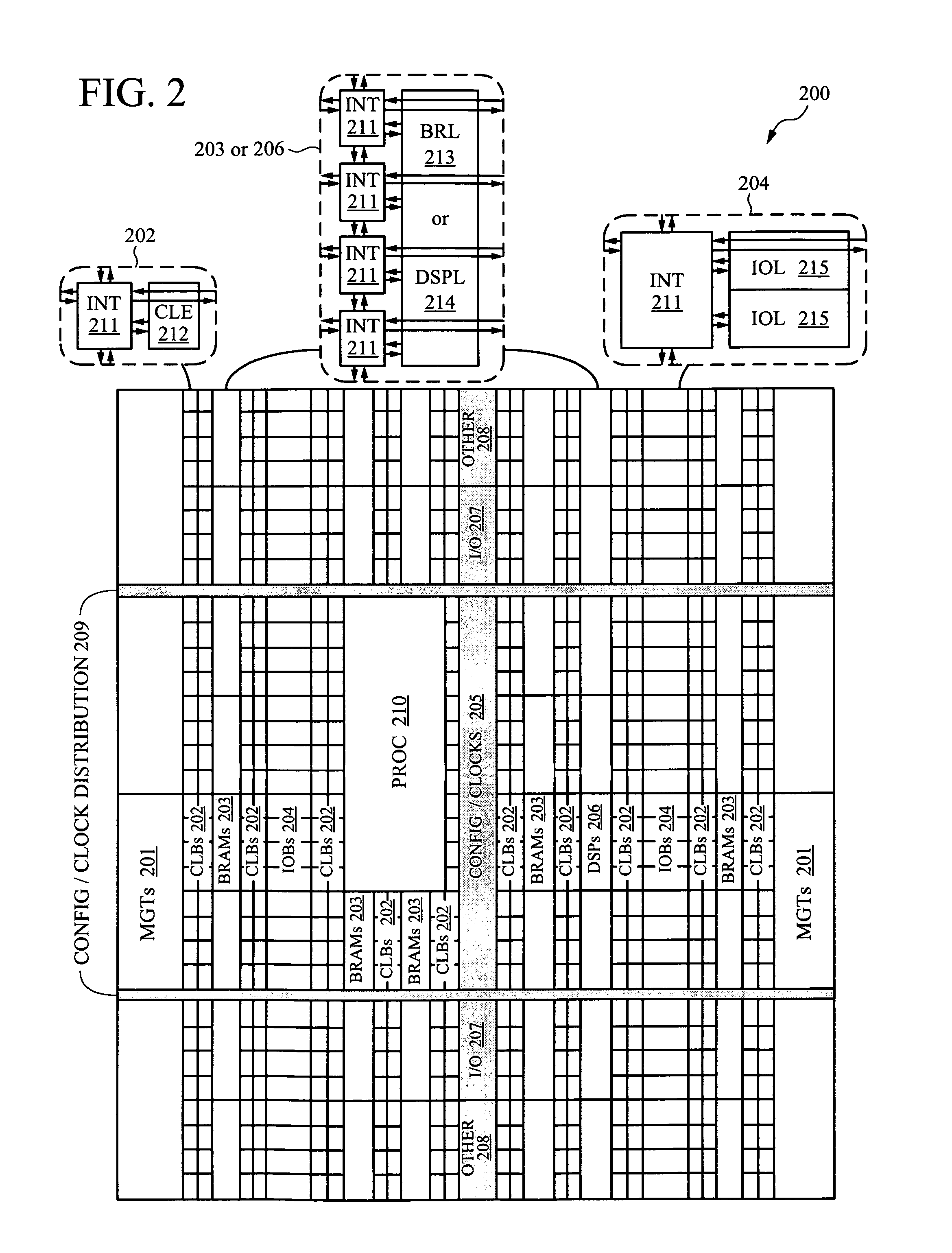
[0028]FIG. 2 illustrates an FPGA architecture 200 suitable for implementing embodiments of the invention. The FPGA architecture 200 includes a large number of different programmable tiles including multi-gigabit transceivers (MGTs 201), configurable logic blocks (CLBs 202), random access memory blocks (BRAMs 203), input / output blocks (IOBs 204), configuration and clocking logic (CONFIG / CLOCKS 205), digital signal processing blocks (DSPs 206), specialized input / output blocks (I / O 207) (e.g., configuration ports and clock ports), and other programmable logic 208 such as digital clock managers, analog-to-digital converters, system monitoring logic, and so forth. Some FPGAs also include dedicated processor blocks (PROC 210).

[0029]In some FPGAs, each programmable tile includes a programmable interconnect element (INT 211) having standardized connections to and from a corresponding interconnect element in each adjacent tile. Therefore, the programmable interconnect elements taken together...


PUM


Abstract

A memory array has a first memory cell with a plurality of transistors connected so as to restore a data value to a node of the memory cell to an initial value following an event upsetting the initial value. A first portion of the plurality of transistors is in a first cell portion and a second portion of the plurality of transistors is in a second cell portion. A second memory cell has a third cell portion and a fourth cell portion. The third cell portion is between the first cell portion and the second cell portion and adjacent to each of the first cell portion and the second cell portion. In a particular embodiment, the memory cell is a single-event-upset (“SEU”) tolerant memory cell and the first and second cell portions are each a half cell of a sixteen transistor memory cell.

Description

FIELD OF THE INVENTION[0001]This invention relates generally to complementary metal-oxide-semiconductor (“CMOS”) memory cells and more particularly to memory cells tolerant to high energy particle (“ion”) hits.BACKGROUND OF THE INVENTION[0002]CMOS circuits are used in a variety of integrated circuit (IC) applications. A CMOS process can be used to fabricate many different sorts of functionality, such as memory, logic, and switching, and thus CMOS techniques are particularly desirable in applications where an IC includes several different types of functional blocks.[0003]One family of ICs employing CMOS fabrication techniques are programmable logic devices (PLDs). PLDs are a well-known type of integrated circuit that can be programmed to perform specified logic functions. One type of PLD, the field programmable gate array (FPGA), typically includes an array of programmable tiles. These programmable tiles can include, for example, input / output blocks (IOBs), configurable logic blocks ...

Claims


Application Information

Patent Timeline
Patent Type & Authority Patents(United States)
IPC IPC(8): G11C11/00
CPCG11C8/04H03K19/00392H03K19/1776H03K19/17764H03K19/1778
Inventor DE JONG, JAN L.NGUYEN, SUSAN XUANPANG, RAYMOND C.
Owner XILINX INC
Why Eureka
Try Eureka