Planar filter, semiconductor device and radio unit
a semiconductor device and filter technology, applied in the field of planar filters, can solve the problems of increasing the loss in the pass band and the area to be occupied by the filter, deteriorating the space efficiency of the ic chip, and increasing the dead space not available, so as to facilitate the fabrication of a semiconductor device, and reduce the cost of semiconductor devices.
- Summary
- Abstract
- Description
- Claims
- Application Information
AI Technical Summary
Benefits of technology
Problems solved by technology
Method used
Image
Examples
first embodiment
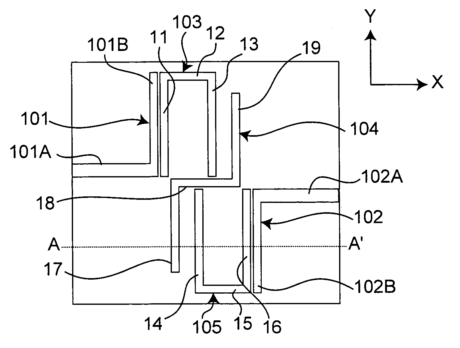
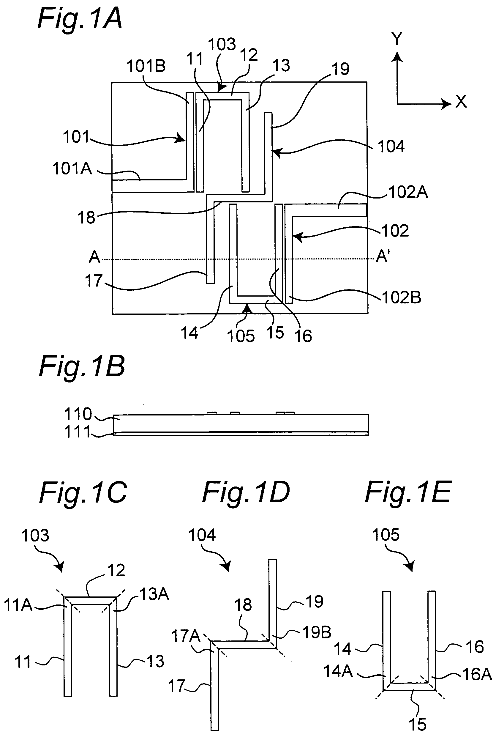
[0029]FIGS. 1A and 1B show a planar filter in the first embodiment of the present invention. FIG. 1A is a plan view, and FIG. 1B is a cross sectional view taken along line A-A′ in FIG. 1A. As shown in FIG. 1A, the planar filter in the first embodiment has a first input / output transmission line 101 serving as an input line, a second input / output transmission line 102 serving as an output line, a first U-shaped open transmission line resonator 103, a second U-shaped open transmission line resonator 105 and a crank-shaped open transmission line resonator 104, which are formed on a dielectric substrate 110. As shown in FIG. 1B, the dielectric substrate 110 has a grounding conductor 111 on its back face.
[0030]As shown in FIG. 1C, the first U-shaped open transmission line resonator 103 has bends so as to be in generally U shape, and is composed of three contiguous connected transmission lines 11, 12 and 13. The transmission lines 11 and 13 face each other in an almost parallel state, and ...
second embodiment
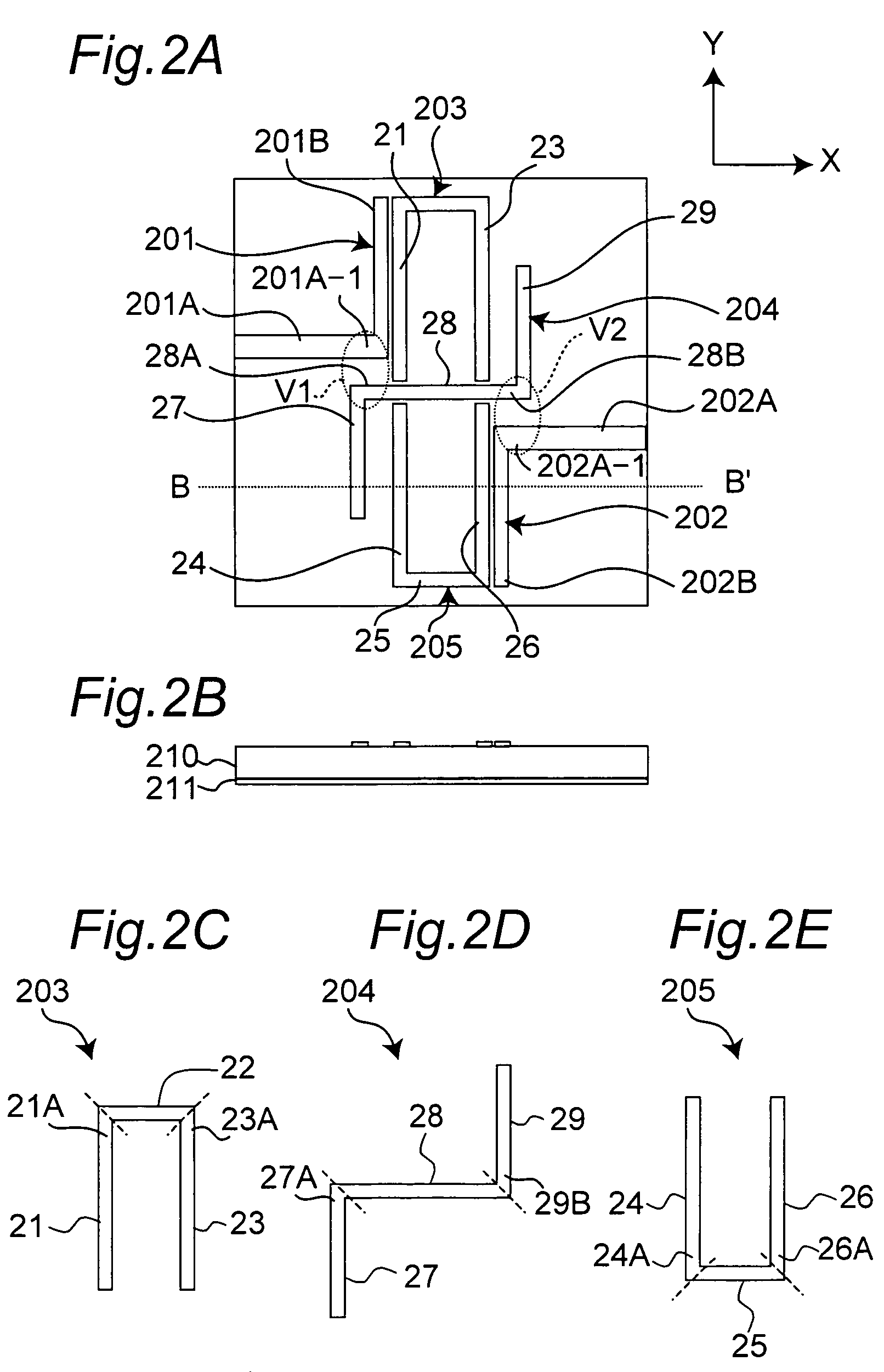
[0045]FIGS. 2A and 2B show a planar filter in the second embodiment of the present invention. FIG. 2A is a plan view, and FIG. 2B is a cross sectional view taken along line B-B′ in FIG. 2A.
[0046]The planar filter in the second embodiment has a first input / output transmission line 201 serving as an input line, a second input / output transmission line 202 serving as an output line, a first U-shaped open transmission line resonator 203, a second U-shaped open transmission line resonator 205 and a crank-shaped open transmission line resonator 204, which are formed on a semi-insulative gallium arsenide substrate 210 of a thickness of 70 μm. As shown in FIG. 2B, the semi-insulative gallium arsenide substrate 210 has a grounding conductor 211 on its back face.
[0047]As shown in FIG. 2C, the first U-shaped open transmission line resonator 203 has bends so as to be in generally U shape, and is composed of three contiguous connected transmission lines 21, 22 and 23. The transmission lines 21 an...
third embodiment
[0065]Next, FIGS. 4A and 4B show a planar filter-integrated even-harmonic mixer device that is a semiconductor device as a third embodiment of the present invention. FIG. 4A is a plan view and FIG. 4B is a cross sectional view taken along line C-C′ in FIG. 4A. The planar filter-integrated even-harmonic mixer device in the third embodiment is formed by integrating a planar filter 301 according to the second embodiment shown in FIG. 2 with an even-harmonic mixer 300 on a semiconductor substrate.
[0066]The even-harmonic mixer device in the third embodiment is an up-converter even-harmonic mixer device for converting an intermediate-frequency signal to a high-frequency signal. The mixer device receives an intermediate-frequency signal (having a frequency (fIF)) and a local oscillation signal (having a frequency (fLO)), and mixes the intermediate-frequency signal and the local oscillation signal to output a high-frequency signal (having a frequency (fRF)). The frequency (fIF), the frequen...
PUM
 Abstract
Description
Claims
Application Information
 - R&D
- Intellectual Property
- Life Sciences
- Materials
- Tech Scout
- Unparalleled Data Quality
- Higher Quality Content
- 60% Fewer Hallucinations
Browse by: Latest US Patents, China's latest patents, Technical Efficacy Thesaurus, Application Domain, Technology Topic, Popular Technical Reports.
© 2025 PatSnap. All rights reserved.Legal|Privacy policy|Modern Slavery Act Transparency Statement|Sitemap|About US| Contact US: help@patsnap.com


