Profile adjustment in plasma ion implanter

a plasma ion implanter and profile adjustment technology, applied in the field of profile adjustment of plasma ion implanters, can solve the problems of contamination of other equipment, poor dose uniformity and dose measurement, and non-repeatability of doses, and achieve the effect of maximizing the retained dose and near surface concentration, and minimizing the spread of dopan

Active Publication Date: 2009-05-05
VARIAN SEMICON EQUIP ASSOC INC
View PDF13 Cites 9 Cited by
  • Summary
  • Abstract
  • Description
  • Claims
  • Application Information

AI Technical Summary

Benefits of technology

[0008]The invention includes methods and apparatuses for providing a dopant profile adjustment solution in plasma doping systems for meeting both concentration and junction depth requirements. Bias ramping and bias ramp rate adjusting may be performed to achieve a desired dopant profile so that shallow and abrupt junction in vertical and lateral directions are realized that are critical to device scaling in plasma doping systems. The ramping of the implanting voltage bias may be linear or non-linear ramping. The rate of ramping the implanting voltage bias may be adjusted and the rate may vary with respect to the deposition rate. Specifically, the rate of ramping the implanting voltage bias may be faster, slower or match the deposition rate. The implanting voltage bias may be ramped in combination with ramping the duty cycle and in combination with changing at least one implant process parameter. The ramping and adjustments are performed to maximize the retained dose and near surface concentration while minimizing dopant spread in vertical and lateral directions.
[0009]A first aspect of the invention is directed to a method for plasma implantation of a workpiece comprising the steps of introducing a dopant gas into a plasma doping chamber and ramping an implanting voltage bias to accelerate the dopant gas ions toward the workpiece. The implanting voltage bias is ramped to maximize the retained dose and near surface concentration of the implanted dopant gas ions into the workpiece.
[0010]A second aspect of the invention is directed to a plasma doping apparatus comprising a plasma doping chamber, a platen, a gas source and a voltage source for implanting dopant gas ions into a workpiece. The voltage source generates an implanting voltage bias to accelerate the dopant gas ions from the plasma toward the workpiece that is ramped to maximize the retained dose and near surface concentration of the implanted dopant gas ions into the workpiece.

Problems solved by technology

These deposited surface layers can cause a number of problems, including dose non-repeatability, poor dose uniformity and dose measurement problems.
In addition, the deposited surface layers can cause contamination of other equipment, such as annealers, when the wafers are subsequently processed in such equipment.

Method used


Image

  • Profile adjustment in plasma ion implanter
  • Profile adjustment in plasma ion implanter
  • Profile adjustment in plasma ion implanter

Examples


Embodiment Construction

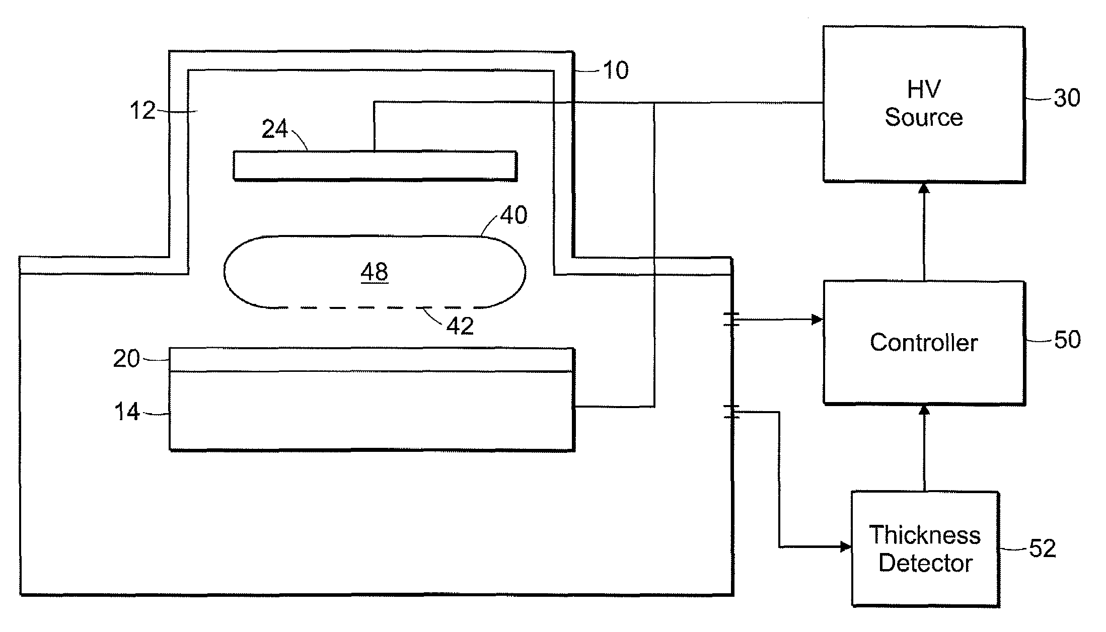
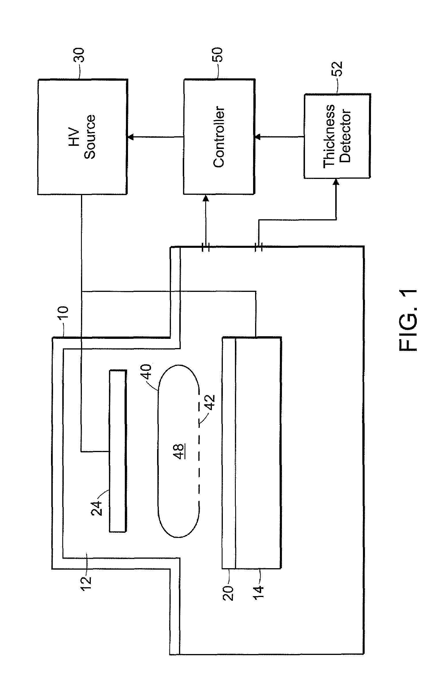
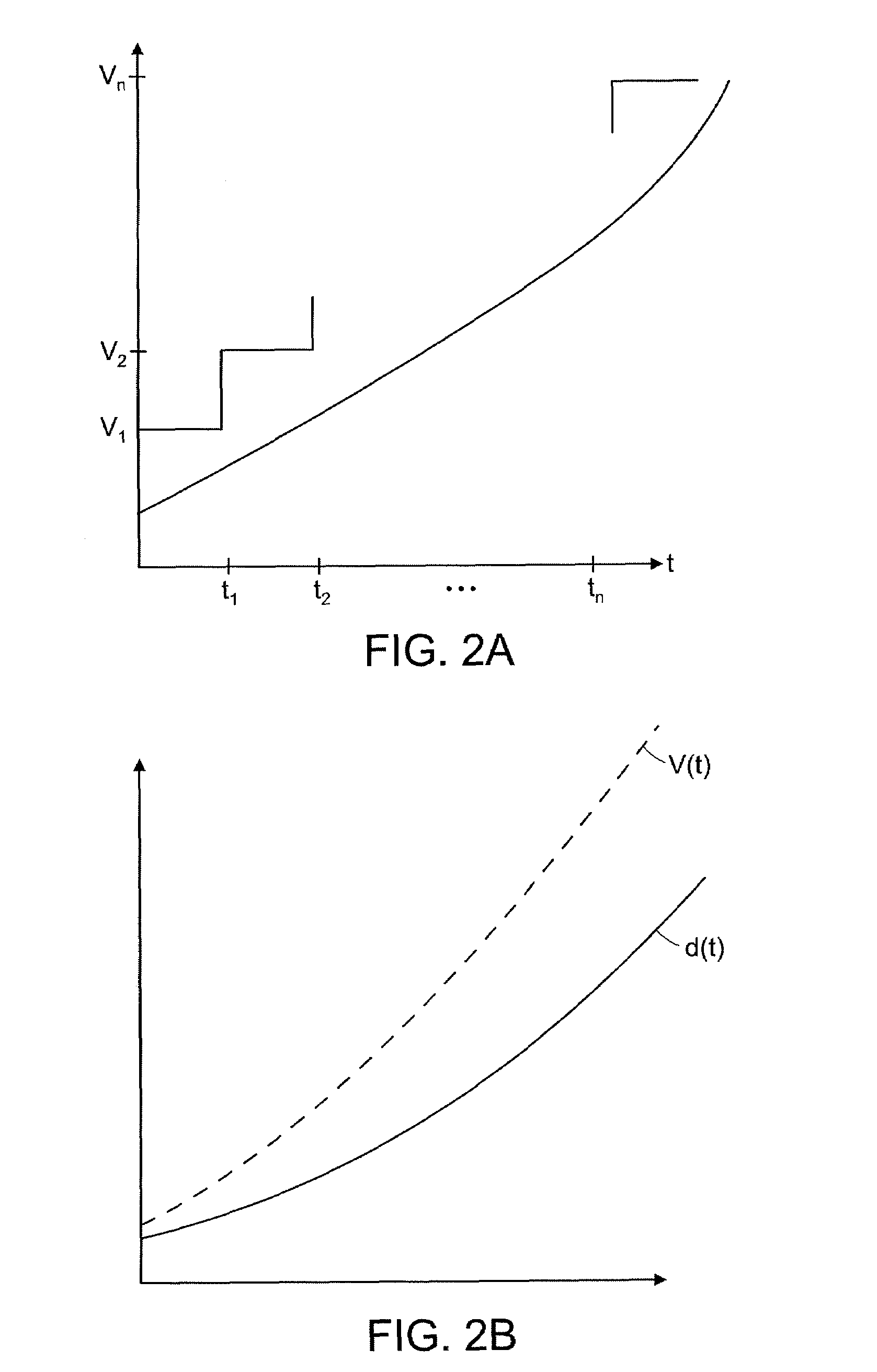
[0021]A box-shape dopant profile is desirable in ion implantation processes for semiconductor device manufacturing. For mono-energetic incident ions, such as those from a beamline implanter, the dopant profile is typically Gaussian. PLAD profiles tend to peak near the surface, with the tail of its profile approaching the beamline tail of the same implant energy. In applications where a certain profile shape is desired, profile adjustment can be made by changing implant energy and dose. In PLAD applications, surface deposition may occur during the implant and by applying a bias voltage that changes with deposition thickness a box-like profile may be achieved. According to one embodiment of the present invention, a method is described to control the ramping and / or rate of ramping the bias voltage in PLAD applications to maximize retained dose and near surface concentration, while minimizing dopant spread in vertical and lateral directions.

[0022]During plasma implant processes, deposit...


PUM


Abstract

A method and apparatus are directed to providing a dopant profile adjustment solution in plasma doping systems for meeting both concentration and junction depth requirements. Bias ramping and bias ramp rate adjusting may be performed to achieve a desired dopant profile so that shallow and abrupt junctions in vertical and lateral directions are realized that are critical to device scaling in plasma doping systems.

Description

RELATED APPLICATIONS[0001]This application claims priority to U.S. Provisional Application No. 60 / 662,018, entitled “PROFILE ADJUSTMENT IN PLASMA ION IMPLANTATION,” filed on Mar. 15, 2005 the contents of which are herein incorporated by reference in their entirety.BACKGROUND OF THE INVENTION[0002]1. Technical Field[0003]The described apparatus and methods relate generally to providing profile adjustment solutions in plasma doping (PLAD) applications to meet both concentration and junction depth requirements. More particularly, the described apparatus and methods are directed to providing abrupt junctions in vertical and lateral directions which are critical to device scaling needs.[0004]2. Background of the Invention[0005]Plasma doping systems are known and used for forming shallow junctions in semiconductor wafers and for other applications requiring high current with relatively low energy ions. In plasma doping systems, a semiconductor wafer is placed on a conductive platen, which...

Claims


Application Information

Patent Timeline
Patent Type & Authority Patents(United States)
IPC IPC(8): H01J37/244
CPCH01J37/3171H01J37/32412H01J37/3299H01J2237/31705H01J37/08H01J37/32H01J37/36
Inventor FANG, ZIWEIAPPEL, RICHARDDENO, VINCENTSINGH, VIKRAMPERSING, HAROLD M.
Owner VARIAN SEMICON EQUIP ASSOC INC
Why Eureka
Try Eureka