Field-effect transistor with spin-dependent transmission characteristics and non-volatile memory using the same

a field-effect transistor and transmission characteristic technology, applied in the field of transistors, can solve the problems of difficult high-density integration of both components, and achieve the effects of high speed, large voltage drop, and high precision

Inactive Publication Date: 2009-05-05
JAPAN SCI & TECH CORP +1
View PDF18 Cites 6 Cited by
  • Summary
  • Abstract
  • Description
  • Claims
  • Application Information

AI Technical Summary

Benefits of technology

[0010]The TMR ratio in a MTJ greatly depends on the bias voltage to be applied to the MTJ, and rapidly decreases according to the bias voltage. When a high driving current is applied to the MTJ to read information with high precision and at a high speed, the voltage drop becomes large in the MTJ, and the TMR ratio decreases accordingly. Therefore, bias resistance is required for the TMR ratio, so as to prevent the TMR ratio from decreasing even if a large voltage drop is caused in the MTJ.

Problems solved by technology

However, if minute MTJs are integrated in conformity with such minute transistors, the contacts and multilayer lines take up a large portion of the cell area, and high-density integration of both components becomes difficult.

Method used


Image

  • Field-effect transistor with spin-dependent transmission characteristics and non-volatile memory using the same
  • Field-effect transistor with spin-dependent transmission characteristics and non-volatile memory using the same
  • Field-effect transistor with spin-dependent transmission characteristics and non-volatile memory using the same

Examples


first embodiment

[0044]First, a MISFET in accordance with the present invention is described, with reference to the accompanying drawings.

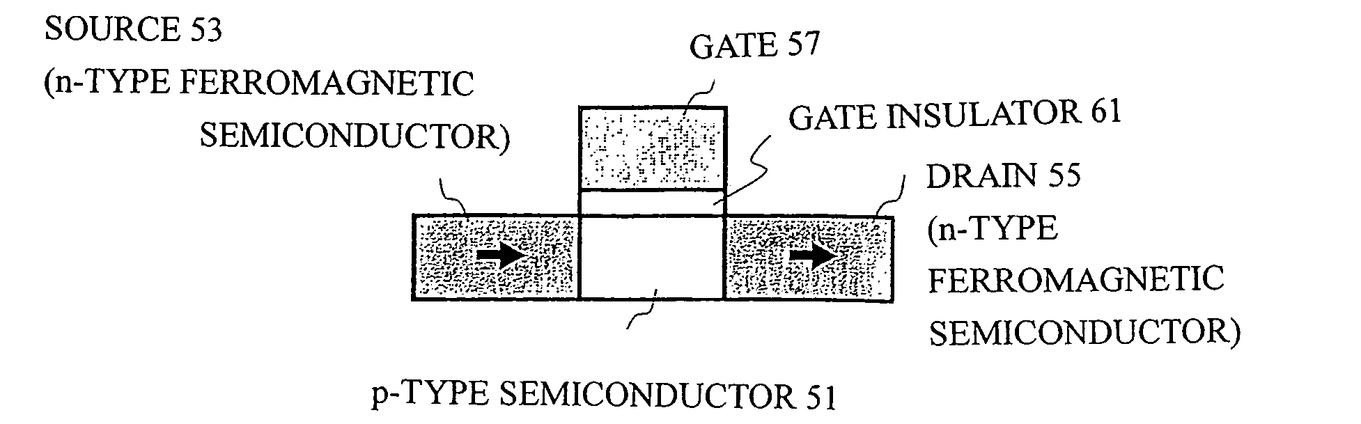
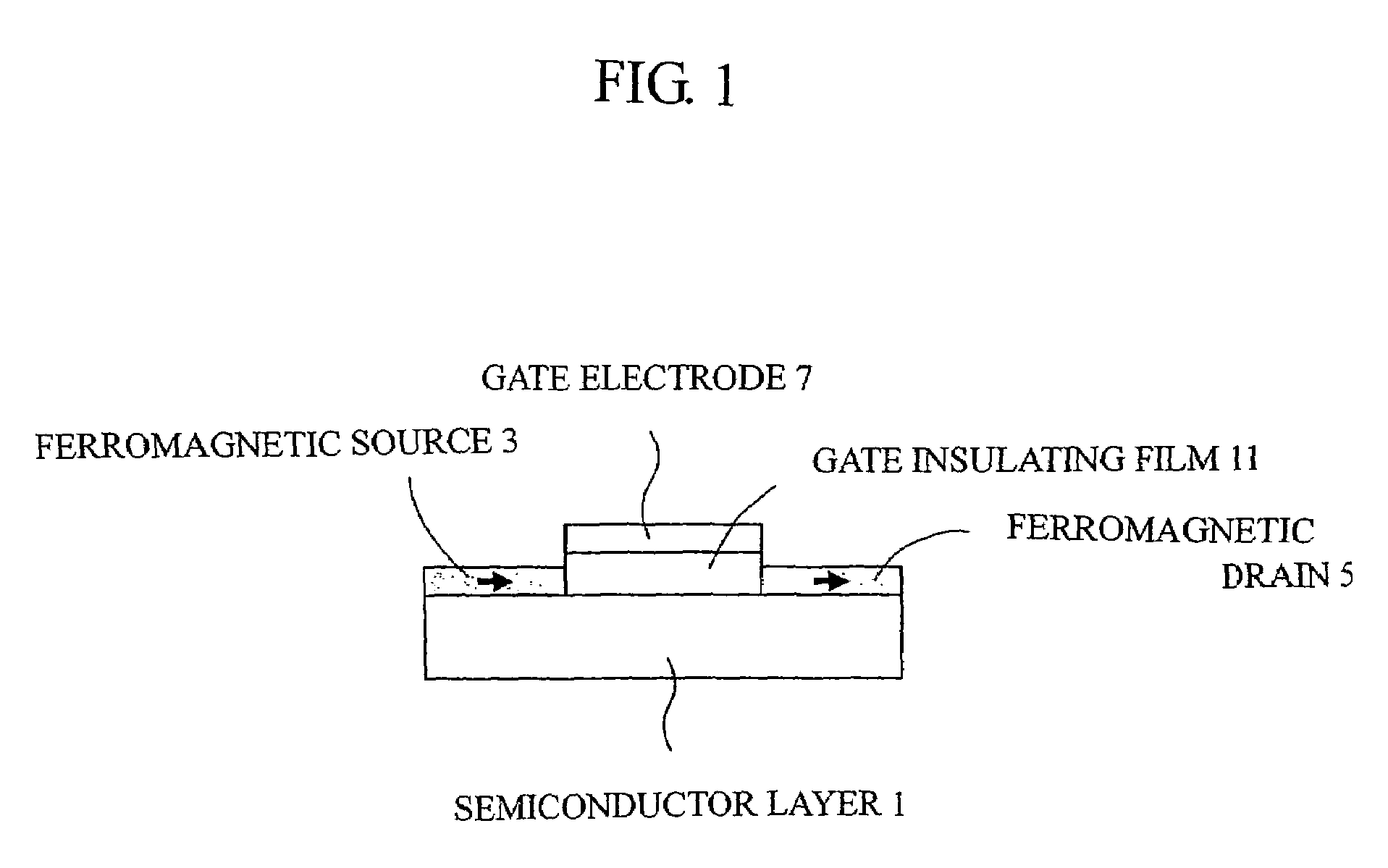
[0045]FIG. 1 is a cross-sectional view of the MISFET in accordance with the first embodiment of the present invention. As shown in FIG. 1, the MISFET of this embodiment includes a MIS structure that is the same as that of a general MISFET (a SiMOSFET, for example) that is formed with a gate electrode 7, a gate insulating film 11, and a non-magnetic semiconductor layer 1, and a source (a ferromagnetic source) 3 and a drain (a ferromagnetic drain) 5 that form a Schottky junction with the non-magnetic semiconductor film 1. The ferromagnetic source and the ferromagnetic drain may be made of: a ferromagnetic metal such as Fe, Ni, Co, Permalloy, CoFe alloy (CO1-xFex), and CoFeB alloy (Co1-x-yFexBy); or a half metal such as Heusler alloy such as CO2MnSi, zinc-blende CrAs, CrSb, and MnAs. Alternatively, the ferromagnetic source and the ferromagnetic drain may be formed wi...

second embodiment

[0052]Next, a MISFET in accordance with the present invention is described, with reference to the accompanying drawings.

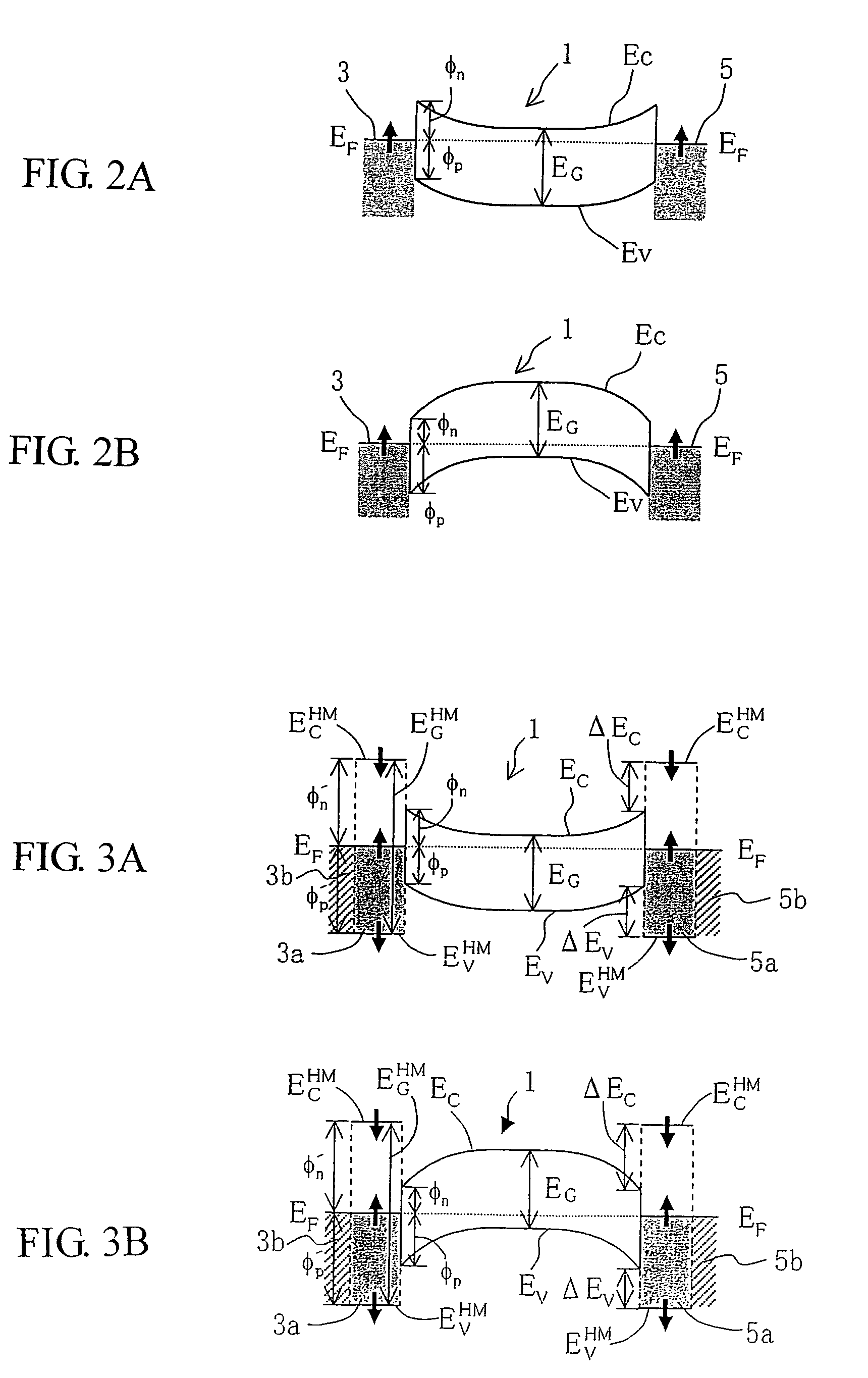
[0053]FIG. 3A illustrates a MISFET in accordance with this embodiment, and shows the energy band structure in the vicinity of the channel region of a MISFET of the accumulation n-channel type in the case where a half metal is used for the ferromagnetic source and the ferromagnetic drain. A half metal exhibits a metallic band structure (hereinafter referred to as the “metallic spin band”) for one direction of spins, while exhibiting a semiconductor (or insulating) band structure (hereinafter referred to as the “semiconductor spin band”) for the opposite spins. With a half metal, a half-occupied band for one spin is provided, and a fully-occupied band (a valence band) is separated for the other spin from an empty band (a conduction band) by a band gap. Accordingly, the Fermi energy EF crosses the metallic spin band of one spin, but crosses the band gap with respect t...

third embodiment

[0088]Next, a MISFET in accordance with the present invention is described in conjunction with the accompanying drawings. In a MISFET in accordance with this embodiment, the ferromagnetic source and the ferromagnetic drain form Schottky junctions with a semiconductor layer and a thin metal layer with a height desired for a barrier. A ferromagnetic metal or a half metal is formed on the metal layer. FIG. 12 shows an energy band structure of a MISFET in accordance with this embodiment. As shown in FIG. 12, the MISFET in accordance with this embodiment has ferromagnetic metal members 23 and 25 as a source and a drain, and thin metal layers 23a and 25a introduced at the interfaces between a semiconductor layer and the ferromagnetic metal members 23a and 25a. The thin metal layers 23a and 25a are used to control the barrier height. Schottky junctions of the metal layers 23a and 25a and the semiconductor layer 21 with which a desired barrier height φn can be obtained are first formed, and...


PUM


Abstract

When a gate voltage VGS is applied, the Schottky barrier width due to the metallic spin band in the ferromagnetic source is decreased, and up-spin electrons from the metallic spin band are tunnel-injected into the channel region. However, down-spin electrons from the nonmagnetic contact (3b) are not injected because of the energy barrier due to semiconductive spin band of the ferromagnetic source (3a). That is, only up-spin electrons are injected into the channel layer from the ferromagnetic source (3a). If the ferromagnetic source (3a) and the ferromagnetic drain (5a) are parallel magnetized, up-spin electrons are conducted through the metallic spin band of the ferromagnetic drain to become the drain current. Contrarily, if the ferromagnetic source (3a) and the (ferromagnetic drain (5a) are antiparallel magnetized, up-spin electrons cannot be conducted through the ferromagnetic drain (5a) because of the energy barrier Ec due to the semiconductive spin band in the ferromagnetic drain (5a). Thus, a high-performance high-degree of integration nonvolatile memory composed of MISFETs operating on the above operating principle can be fabricated.

Description

FIELD OF THE INVENTION[0001]The present invention relates to novel transistors, and more particularly, to a field-effect transistor with spin-dependent transmission characteristics and a non-volatile memory using the field-effect transistor.BACKGROUND OF THE INVENTION[0002]Today's highly advanced information society has dramatically developed, and particularly, “mobile communication devices” are being widely spread in the general public. The great demand for “mobile communication devices” is regarded as one of the essential elements in the future semiconductor industry. To satisfy the demand, however, it is necessary to achieve non-volatility of information, as well as high-speed performance, lower electric consumption, and large capacities that have conventionally be required in semiconductor integrated circuits. In response to such demands, attention has been drawn to a novel memory device in which the ferromagnetic storage technique that excels in non-volatile high-density record...

Claims


Application Information

Patent Timeline
Patent Type & Authority Patents(United States)
IPC IPC(8): H01L29/78G11C11/16H01L21/8246H01L27/22H01L29/66
CPCB82Y10/00H01L29/66984H01L27/228G11C11/16H01L29/47G11C11/161H10B61/22H01L29/82H01L27/105
Inventor SUGAHARA, SATOSHITANAKA, MASAAKI
Owner JAPAN SCI & TECH CORP
Why Eureka
Try Eureka