Eureka AIR delivers breakthrough ideas for toughest innovation challenges, trusted by R&D personnel around the world.

Embedded microprocessor for integrated circuit testing and debugging

Active Publication Date: 2009-05-26
TAHOE RES LTD
View PDF69 Cites 22 Cited by
  • Summary
  • Abstract
  • Description
  • Claims
  • Application Information

AI Technical Summary

Benefits of technology

[0010]It is realized that as integrated circuit features become smaller and smaller, it becomes less expensive to place a microprocessor on a chip. While in the past it might have been too expensive to place a microprocessor on a chip just for testing or debugging, it is now more cost effective to place a microprocessor on a chip just for testing and debugging. The result is faster testing and debugging, or more testing and debugging coverage of the device in the same amount of time. More analysis can be performed in the same amount of time resulting in higher quality devices.
[0011]With an embedded processor right on the chip, tests, patterns, simulation, etc., may be run right on the device. Because no communication is needed from the chip to the outside world for controlling the testing or debugging, the bottleneck of a serial interface is avoided.
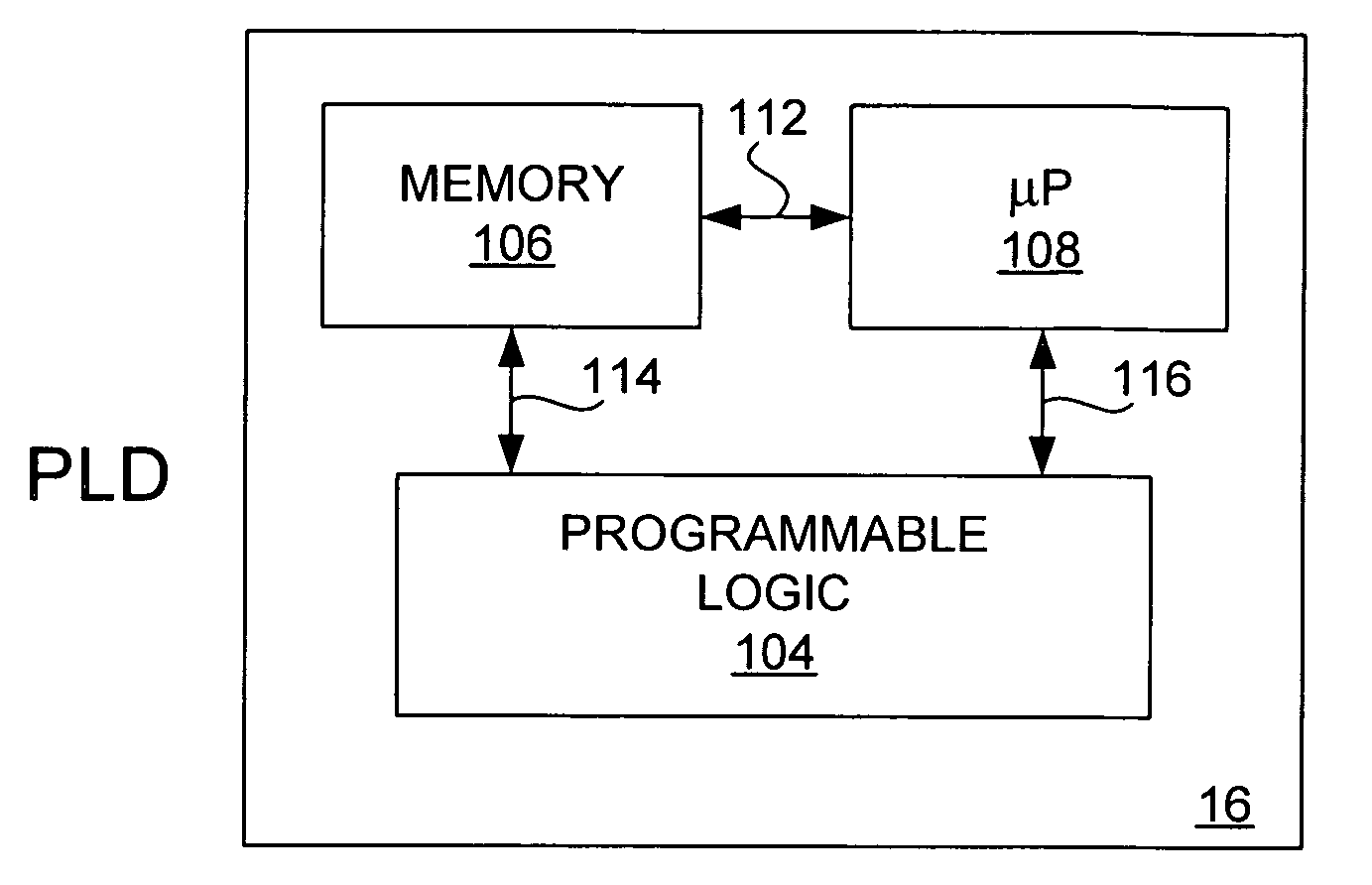
[0012]In one embodiment for integrated circuit testing, an embedded microprocessor core is present in the PLD. Test costs are reduced and test coverage is increased, for example, by running through a regression that tests all hard function blocks and then reports status back through a JTAG port, SPI or other port.
[0013]In a second embodiment for debugging, an embedded microprocessor core in the PLD aids in the real-time debugging of the system at frequency. The embedded microprocessor is also useful for failure analysis probing of failed systems. Further, the embedded microprocessor can be used to improve the performance of gathering probe data during debugging. Further, the embedded microprocessor gives selective feedback by using enhanced compression techniques, adaptive selection of data based on known patterns and routines, and wider parallel output of data versus using a serial JTAG port interface.

Problems solved by technology

But, as integrated circuits become more and more complex, testing costs become higher and higher.
The time and effort involved in testing these PLDs before they are sold to a customer is increasing.
Likewise, the complexity of newer PLDs means that it takes more time and effort for a design engineer to debug a PLD.
Although the above techniques are useful, the increasing complexity of integrated circuits slows the speed at which testing and debugging of integrated circuits can occur.
For example, during hardware emulation on chip, testing or debugging may be slow.
Testing or debugging is slow because of the speed of the external computer being used, the serial port on the device through which data and patterns must be passed, the necessary data gathering on the chip itself, and the presence of any probes used in the device.
These emulation machines though, are extremely expensive.
A software simulation of an integrated circuit is also effected by increasing device complexity.
Because the simulation model might be inaccurate, extensive testing is needed.
Further, the host computer itself may be slow.
Thus, the more complex the device, the slower the simulation goes.

Method used


Image

  • Embedded microprocessor for integrated circuit testing and debugging
  • Embedded microprocessor for integrated circuit testing and debugging
  • Embedded microprocessor for integrated circuit testing and debugging

Examples


Embodiment Construction

[0023]The present invention is applicable to both the testing and debugging of integrated circuits (devices). Testing of an integrated circuit is performed by the device manufacturer before the device is shipped to a customer, and typically uses a test system. Debugging of the device is performed by the customer who has placed their design onto the device, and who desires to check its functionality before shipping it out as a final product. Debugging is typically controlled by a customer host computer, as is known in the art. In order to develop an electronic design for programming a hardware device, a programmable logic development system is used. As explained above, the present invention is applicable to many types of integrated circuits; the below discussion refers to a “PLD” for ease of explanation.

Programmable Logic Development System

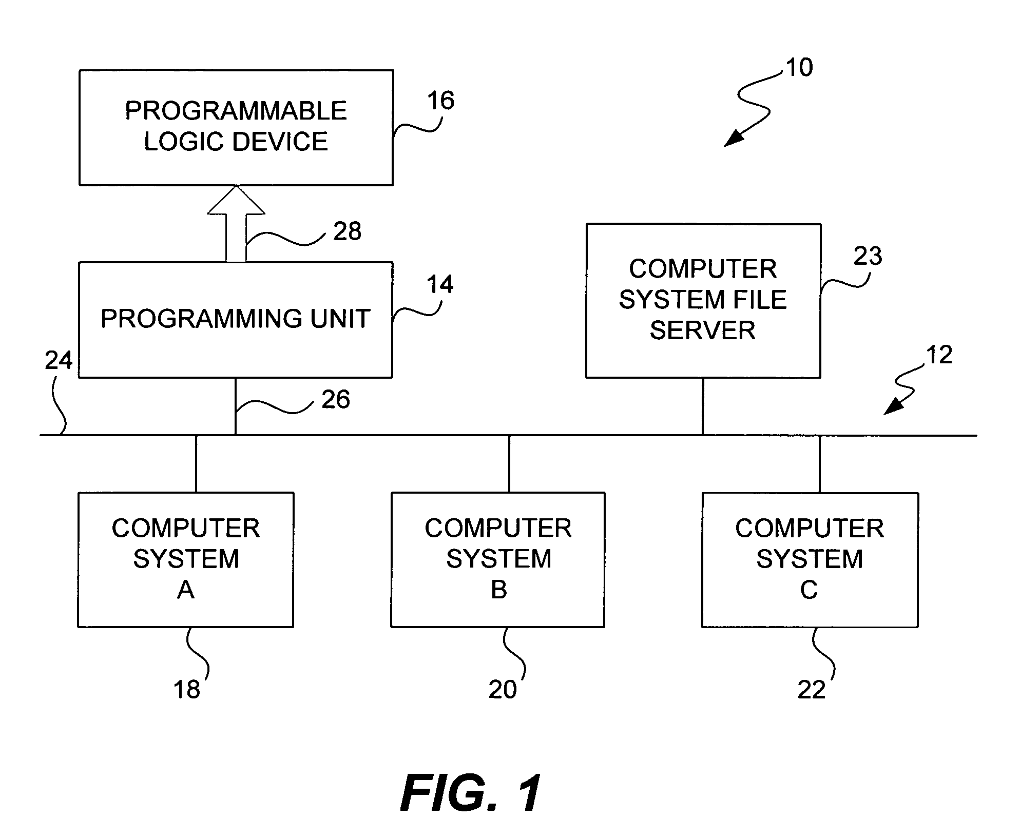
[0024]FIG. 1 is a block diagram of an embodiment of a programmable logic development system 10 that includes a computer network 12, a programming ...


PUM


Abstract

A technique for embedding a microprocessor into an integrated circuit allows on-chip testing and debugging. The microprocessor present on the chip tests and debugs the rest of the chip. Both testing and debugging of a programmable logic device use an embedded microprocessor. Testing is performed by the device manufacturer using a test system. Debugging is performed by a user using a host computer. A PLD includes programmable logic, an embedded microprocessor and separate memory. Testing or debugging routines, patterns, simulations, etc., are downloaded onto the memory. The microprocessor executes the test or debug routine and uploads results to the test system or host computer. The technique is applicable any integrated circuit that can include an embedded microprocessor and associated memory, such as a PLD, an ASIC, a memory chip, or an analog chip.

Description

FIELD OF THE INVENTION[0001]The present invention relates generally to testing and debugging of integrated circuits. More specifically, the present invention relates to a technique of using an embedded microprocessor for such testing and debugging.BACKGROUND OF THE INVENTION[0002]In the field of electronics various electronic design automation (EDA) tools are useful for automating the process by which integrated circuits, multi-chip modules, boards, etc., are designed and manufactured. In particular, electronic design automation tools are useful in the design of standard integrated circuits, custom integrated circuits (e.g., ASICs), and in the design of custom configurations for programmable integrated circuits. Integrated circuits that may be programmable by a customer to produce a custom design for that customer include programmable logic devices (PLDs). Programmable logic devices refer to any integrated circuit that may be programmed to perform a desired function and include prog...

Claims


Application Information

Patent Timeline
IPC IPC(8): G06F11/00
CPCG01R31/31705G06F11/27G11C29/16G11C29/56
Inventor PLOFSKY, JORDAN
Owner TAHOE RES LTD
Why Eureka
Eureka Blog
Learn More