Phase-shifting circuit and multibit phase shifter

a phase shifter and circuit technology, applied in waveguide devices, network simulating reactances, waveguide type devices, etc., can solve problems such as circuits with a problem of increasing their size, and achieve the effects of reducing the size of inductors, miniaturizing circuits, and low loss

Active Publication Date: 2009-06-02
MITSUBISHI ELECTRIC CORP
View PDF15 Cites 8 Cited by
  • Summary
  • Abstract
  • Description
  • Claims
  • Application Information

AI Technical Summary

Benefits of technology

[0010]This makes it possible to form a bandpass filter circuit and low-pass filter circuit by switching, and to vary the pass phase of the high frequency signal input, thereby being able to obtain a desired phase shift amount at a low loss. In addition, since the phase-shifting circuit employs the low-pass filter, it can reduce the size of the inductors as compared with a conventional example that employs a high-pass filter, thereby being able to miniaturize itself. Furthermore, since the phase-shifting circuit can be composed of the two switching elements, four inductors, a single capacitor, and a single through hole, it offers an advantage of being able to miniaturize the circuit.

Problems solved by technology

In addition, since the cutoff frequency of the HPF must be lowered with the reduction in the phase shift amount, the circuit has a problem of increasing its size.

Method used


Image

  • Phase-shifting circuit and multibit phase shifter
  • Phase-shifting circuit and multibit phase shifter
  • Phase-shifting circuit and multibit phase shifter

Examples


embodiment 1

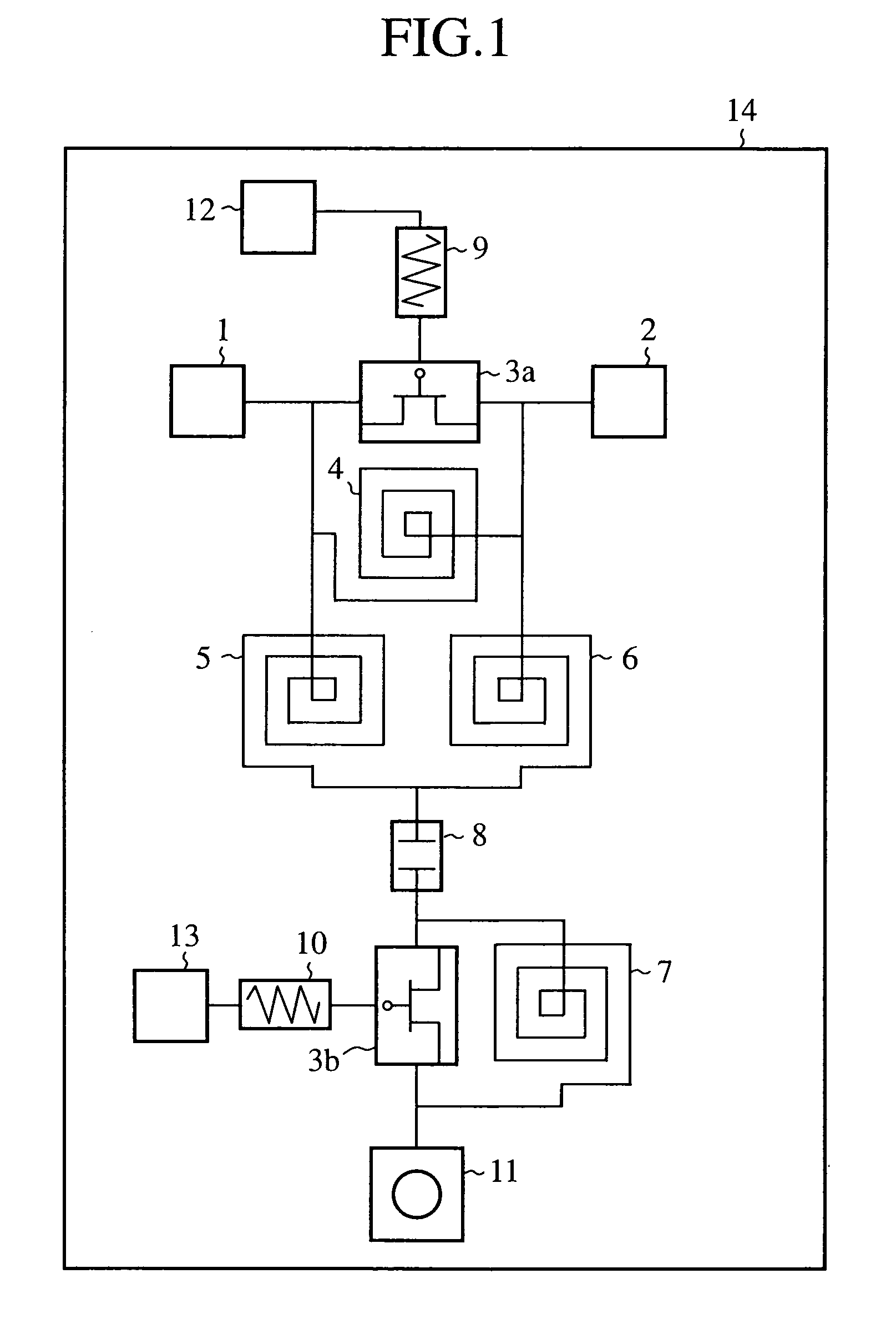
[0042]FIG. 1 is a circuit diagram showing a configuration of the phase-shifting circuit of an embodiment 1 in accordance with the present invention.

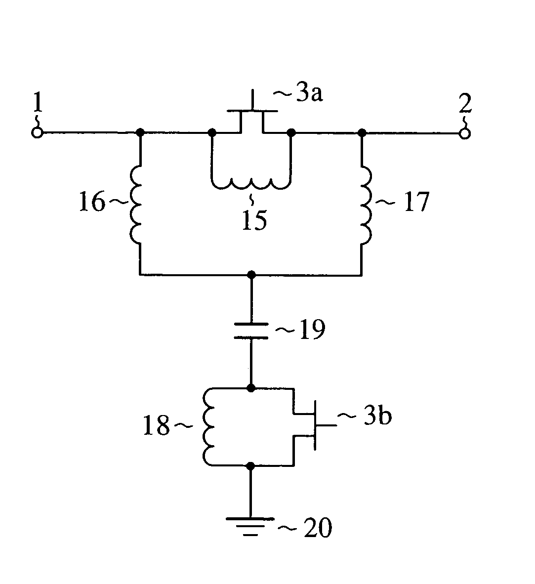
[0043]In FIG. 1, the phase-shifting circuit is formed monolithically on a semiconductor substrate 14. It is configured in such a manner that a parallel circuit (first parallel circuit) composed of an FET (first switching element) 3a and a spiral inductor (first inductor) 4 is connected across a high frequency signal input terminal 1 and an output terminal 2, and that the FET 3a has its gate supplied with a first control signal from an input terminal 12 via a resistor 9. In addition, a series circuit composed of a spiral inductor (second inductor) 5 and a spiral inductor (third inductor) 6 is also connected in parallel with the parallel circuit. The point of connection between the spiral inductor 5 and spiral inductor 6 is connected to a first terminal of an MIM capacitor 8. Between a second terminal of the MIM capacitor 8 and a through h...

embodiment 2

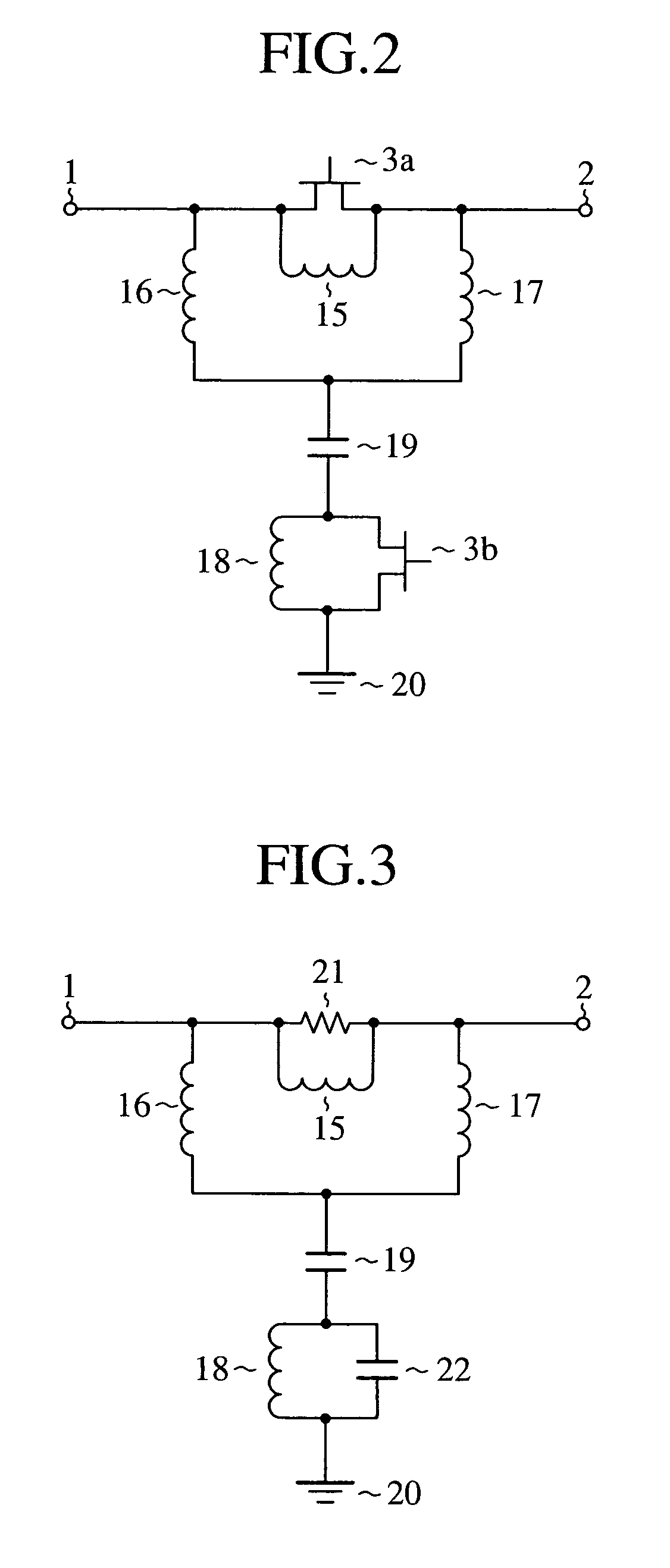
[0052]FIG. 5 is a circuit diagram showing a configuration of the phase-shifting circuit of the embodiment 2 in accordance with the present invention. In FIG. 5, the same or like portions to those of FIG. 2 are designated by the same reference numerals, and duplicate explanation will be omitted basically. The configuration of the phase-shifting circuit includes an FET (third switching element) 25 in place of the capacitor 19 of FIG. 2.

[0053]The FET 25, which operates as a switch for switching the ON / OFF state, carries out the operation in the same manner as the FET 3a and FET 3b in response to the control signal.

[0054]Next, the operation will be described.

[0055]When the control signal sets the FET 3a at the ON state, the FET 3b at the OFF state and the FET 25 at the ON state, the phase-shifting circuit of FIG. 5 is considered to become the equivalent circuit as shown in FIG. 6. In FIG. 6, the same or like components to those of FIG. 3 are designated by the same reference numerals. He...

embodiment 3

[0061]FIG. 8 is a circuit diagram showing a configuration of the phase-shifting circuit of an embodiment 3 in accordance with the present invention. In FIG. 8, the same or like portions to those of FIG. 2 are designated by the same reference numerals, and duplicate explanation will be omitted basically. The configuration of the phase-shifting circuit replaces the parallel circuit composed of the inductor 18 and FET 3b of FIG. 2 by only the FET 3b (second switching element).

[0062]Next, the operation will be described.

[0063]When the control signal sets the FET 3a at the ON state and the FET 3b at the OFF state, the phase-shifting circuit of FIG. 8 can be considered to have an equivalent circuit as shown in FIG. 9. In FIG. 9, the same or like components to those of FIG. 3 are designated by the same reference numerals.

[0064]In the circuit of FIG. 9, the combined capacitance of the capacitor 19 and OFF capacitance 22 is set in such a manner to become nearly an open state. Here, since the...


PUM


Abstract

A phase-shifting circuit includes: a first parallel circuit which is connected across input and output terminals of a high frequency signal, composed of a first inductor and a first switching element that exhibits a through state in an ON state and a capacitive property in an OFF state, and produces parallel resonance at a prescribed frequency when the first switching element is in the OFF state; a series circuit composed of a second inductor and a third inductor and connected in parallel with the first parallel circuit; a capacitor having its first terminal connected to a point of connection of the second and third inductors; and a second parallel circuit which is connected across a second terminal of the capacitor and a ground, composed of a fourth inductor and a second switching element that exhibits a through state in an ON state and a capacitive property in an OFF state, and produces parallel resonance at a prescribed frequency when the second switching element is in the OFF state. The phase-shifting circuit establishes by switching an operation mode of setting the first switching element at the ON state and the second switching element at the OFF state, or an operation mode of setting the first switching element at the OFF state and the second switching element at the ON state.

Description

TECHNICAL FIELD[0001]The present invention relates to a miniature, low-loss phase-shifting circuit and multibit phase shifter.BACKGROUND ART[0002]FIG. 28 is a circuit diagram showing a configuration of a conventional phase-shifting circuit disclosed in C. F. Campbell and S. A. Brown, “A Compact 5-Bit Phase Shifter MMIC for K-Band Satellite Communication Systems”, IEEE IMS2000 Proceedings. In FIG. 28, the phase-shifting circuit includes a high frequency signal input terminal 101, high frequency signal output terminal 102, first field-effect transistor (abbreviated to “FET” from now on) 103, second FET 104, first inductor 105, second inductor 106, third inductor 107, capacitor 108 and ground 109.[0003]In the circuit, the field-effect transistor (abbreviated to “FET” from now on) 103 operates as a switch for switching between an ON state and OFF state. When a voltage equipotential to a drain voltage and source voltage is applied to a gate terminal, the FET 103 enters into an ON state, ...

Claims


Application Information

Patent Timeline
Patent Type & Authority Patents(United States)
IPC IPC(8): H01P9/00
CPCH01P1/185H03H11/20H03H19/008H03H11/48
Inventor MIYAGUCHI, KENICHIHIEDA, MORISHIGENISHINO, TAMOTSUHANGAI, MASATAKEMIYAZAKI, MORIYASUYOSHIDA, YUKIHISATAKAGI, TADASHIHATAMOTO, MIKIO
Owner MITSUBISHI ELECTRIC CORP
Why Eureka
Try Eureka