Method of correlating silicon stress to device instance parameters for circuit simulation

a technology of circuit simulation and silicon stress, applied in the direction of individual semiconductor device testing, semiconductor/solid-state device testing/measurement, instruments, etc., can solve the problems of increasing the amount of oxide in the channel, increasing the cost of prototype integrated circuit design, and increasing the cost of manufacturing. , to achieve the effect of reducing the amount of oxide and reducing the actual stress in the channel

Active Publication Date: 2009-06-02
SYNOPSYS INC
View PDF9 Cites 41 Cited by
  • Summary
  • Abstract
  • Description
  • Claims
  • Application Information

AI Technical Summary

Benefits of technology

[0012]Fourth, the LOD model fails to take into account the presence of other structures in the neighborhood of a region under study, apart from the nearest STI interface. Other structures beyond this interface might reduce the amount of oxide presumed to be exerting a force, and therefore might reduce the actual stress in the channel.

Problems solved by technology

Because the fabrication of prototype integrated circuit designs is expensive and time consuming, it is typical for circuit designers to first simulate their designs using computer simulation tools.
As process technologies have continued to shrink, however, the piezoresistive effect on transistor performance is no longer negligible.
The computation time required to obtain accurate results, however, limited the utility of this kind of analysis to only small regions of a chip layout that include only several transistors.
For example, it has not been practical to perform a TCAD analysis to obtain reasonably accurate circuit level parameters for layout regions larger than about a dozen transistors, or about 2-3 diffusion regions.
Even then, huge amounts of CPU time, up to several hours per transistor, were required to obtain reasonably accurate results.
Even as computing power increases, the required computation time continues to make this approach prohibitively expensive for any large fragments of the chip layout.
Unfortunately, the LOD model has a number of deficiencies.
First, the model is limited to STI-induced stress.
Second, the LOD model fails to take into account stresses that might be present transversely to the length of diffusion, across the channel width-wise.
Third, more generally than the second deficiency, since the LOD model considers only hydrostatic pressure, which is a sum of all normal (i.e. volume changing rather than rotational) stress components, it fails to take into account differing vector stress components.
Fourth, the LOD model fails to take into account the presence of other structures in the neighborhood of a region under study, apart from the nearest STI interface.

Method used


Image

  • Method of correlating silicon stress to device instance parameters for circuit simulation
  • Method of correlating silicon stress to device instance parameters for circuit simulation
  • Method of correlating silicon stress to device instance parameters for circuit simulation

Examples


Embodiment Construction

[0028]The following description is presented to enable any person skilled in the art to make and use the invention, and is provided in the context of a particular application and its requirements. Various modifications to the disclosed embodiments will be readily apparent to those skilled in the art, and the general principles defined herein may be applied to other embodiments and applications without departing from the spirit and scope of the present invention. Thus, the present invention is not intended to be limited to the embodiments shown, but is to be accorded the widest scope consistent with the principles and features disclosed herein.

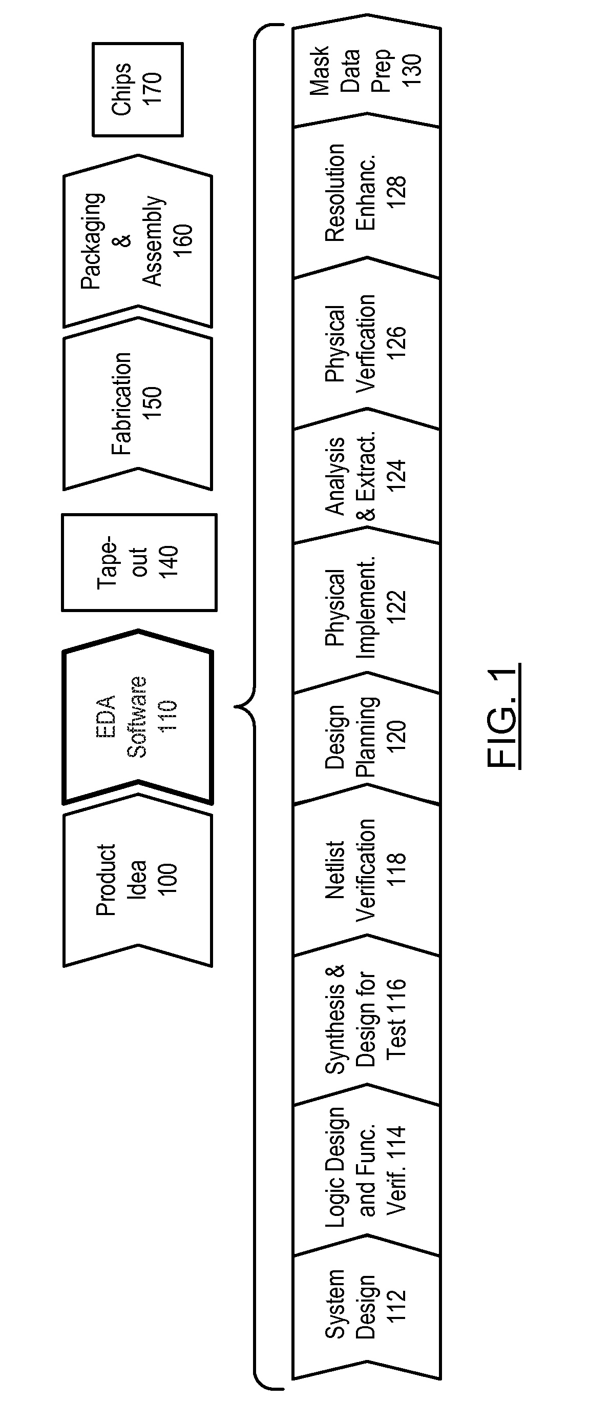
[0029]FIG. 1 shows a simplified representation of an illustrative digital integrated circuit design flow. At a high level, the process starts with the product idea (step 100) and is realized in an EDA (Electronic Design Automation) software design process (step 110). When the design is finalized, it can be taped-out (step 140). After tape out, ...


PUM


Abstract

Roughly described, standard SPICE models can be modified by substituting a different stress analyzer to better model the stress adjusted characteristics of a transistor. A first, standard, stress-sensitive, transistor model is used to develop a mathematical relationship between the first transistor performance measure and one or more instance parameters that are available as inputs to a second, stress-insensitive, transistor model. The second transistor model may for example be the same as the first model, with its stress sensitivity disabled. Thereafter, a substitute stress analyzer can be used to determine a stress-adjusted value for the first performance measure, and the mathematical relationship can be used to convert that value into specific values for the one or more instance parameters. These values are then provided to the second transistor model for use in simulating the characteristics of the particular transistor during circuit simulation.

Description

1. FIELD OF THE INVENTION[0001]The invention relates to circuit simulation techniques, and more particularly to adjustment of device instance parameters in such a simulation to account for stress impacts on transistor performance.2. BACKGROUND AND SUMMARY OF THE INVENTION[0002]Because the fabrication of prototype integrated circuit designs is expensive and time consuming, it is typical for circuit designers to first simulate their designs using computer simulation tools. In this way corrections can be made before the time and expense of prototype fabrication is incurred. One popular family of circuit simulators, especially useful for analog performance verification and behavior prediction, is known generically as SPICE (Simulation Program with Integrated Circuits Emphasis). The family includes the original SPICE program, numerous subsequent versions of the program, and numerous offshoots available from other sources. Circuit simulators are used often for predicting and verifying, am...

Claims


Application Information

Patent Timeline
Patent Type & Authority Patents(United States)
IPC IPC(8): G06F17/50
CPCG06F17/5036G06F30/367
Inventor LIN, XI-WEIMOROZ, VICTORPRAMANIK, DIPANKAR
Owner SYNOPSYS INC
Why Eureka
Try Eureka