Passivation for cleaning a material

a technology of passivation and cleaning material, which is applied in the preparation of detergent mixture compositions, chemistry apparatus and processes, and detergent compositions. it can solve the problems of affecting the electrical communication between the substrate and the conductive material subsequently deposited, and affecting the etching rate of the exposed material at the same rate, so as to achieve the effect of reducing the amount of initial etching of the workpi

Inactive Publication Date: 2009-06-09
MICRON TECH INC
View PDF36 Cites 4 Cited by
  • Summary
  • Abstract
  • Description
  • Claims
  • Application Information

AI Technical Summary

Problems solved by technology

While etching a semiconductor device, more than one type of material included as part of that device may be exposed to the etching environment, although it may not be desirable to etch all of the exposed materials at the same rate.
However, before such a conductive layer is deposited, conditions may be present that would interfere with electrical communication between the silicon substrate and the conductive layer to be deposited.
Accordingly, if any such oxide is allowed to remain at the bottom of the contact, it will hinder electrical communication between the substrate and a subsequently deposited conductive material.
Unfortunately, while HF etches the native oxide from the bottom of the contact, it also etches other oxides, including the deposited BPSG that defines the contact.
Widening the contact is detrimental to semiconductor device fabrication, as the contact may be near conductive structures such as the conductive electrode of a capacitor.
This is even more of a problem if other processes also widen the contact.
Nevertheless, thinning the BPSG may be undesirable in certain circumstances.

Method used


Image

  • Passivation for cleaning a material
  • Passivation for cleaning a material
  • Passivation for cleaning a material

Examples


Embodiment Construction

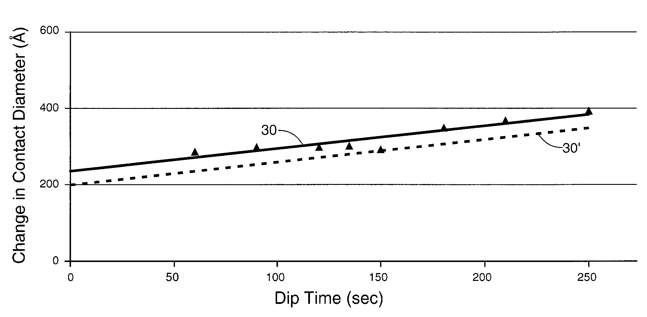
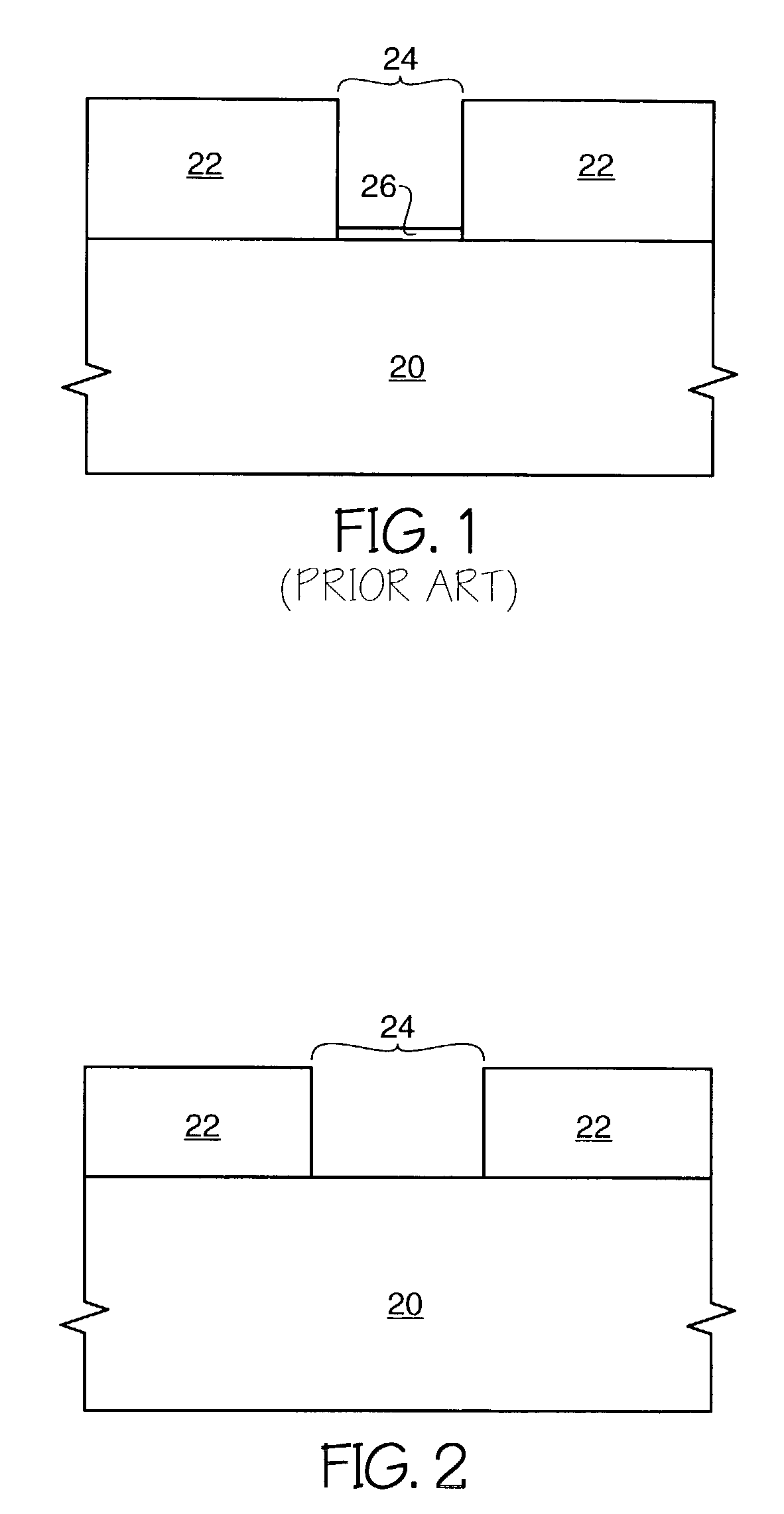
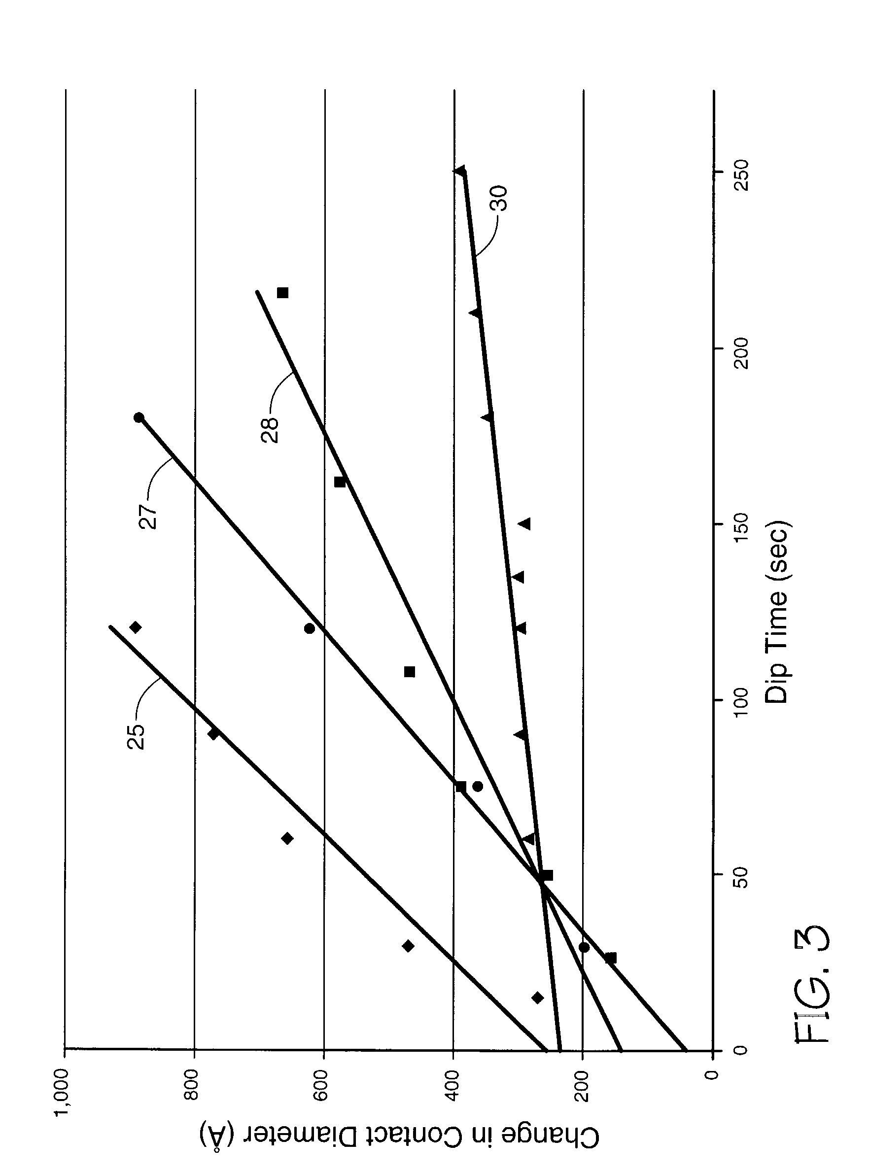
[0019]FIG. 1 depicts an in-process portion of a prior art semiconductor device comprising a silicon substrate 20 supporting a BPSG layer 22. A contact 24 has been etched through the BPSG 22, and a native oxide 26 has been formed from the portion of the silicon substrate 20 exposed by contact 24. Regardless of whether this native oxide 26 is intentionally formed or not, or whether the native oxide 26 is desirable at some point or not, it is assumed that by some step in the fabrication process, it is desired to remove the native oxide 26 with little if any effect on the BPSG. This result is pictured in FIG. 2. The effect of prior art attempts to achieve this result can be seen in the graph of FIG. 3. That figure displays the effect of various contact cleaning chemistries (CCS) in terms of the change in contact diameter as a function of the amount of time the silicon substrate remains dipped in a particular chemistry. The change in contact diameter (ΔCD) is measured along the Y-axis in...


PUM

PropertyMeasurementUnit
diameteraaaaaaaaaa
diameteraaaaaaaaaa
contact diameteraaaaaaaaaa

Abstract

A contact is defined by an opening etched into borophosphosilicate glass (BPSG) down to a silicon substrate. In a contact cleaning process designed to remove native oxide at the bottom of the contact with little effect on the BPSG, the contact is dipped in an etch retardant before being dipped in a cleaning solution containing both the etch retardant and an etchant. The dip in etch retardant modifies the surface of the BPSG, thereby lessening the enhanced etching experienced during the initiation of the dip into the etchant / etch retardant cleaning solution. Results of a etchant / etch retardant clean, both with and without the prepassivation, can be illustrated on a graph depicting the change in contact diameter as a function of dip time. Specifically, the results define “best fit” lines on that graph. For a given dip time, a first line representing the prepassivation+etchant / etch retardant clean is 30 to 40 Angstroms lower than a second line representing the prior art clean using the etchant / etch retardant without prepassivation. Accordingly, the first line's Y-axis intercept, representing the “zero dip time,” is also 30 to 40 Angstroms lower than the second line's zero dip time.

Description

RELATED APPLICATION[0001]This application is a divisional of U.S. application Ser. No. 09 / 477,299, filed Jan. 4, 2000, now U.S. Pat. No. 6,531,071.TECHNICAL FIELD[0002]The present invention relates generally to cleaning methods used in the fabrication of semiconductor devices. More particularly, the present invention pertains to protecting at least one material while removing at least one other material from a workpiece during the fabrication of a semiconductor device.BACKGROUND OF THE INVENTION[0003]The fabrication of semiconductor devices often involves providing materials over a substrate and shaping those materials through processes such as photolithography and etching. In the current application, the term “substrate” or “semiconductor substrate” will be understood to mean any construction comprising semiconductor material, including but not limited to bulk semiconductive materials such as a semiconductor wafer (either alone or in assemblies comprising other materials thereon), ...

Claims


Application Information

Patent Timeline
Patent Type & Authority Patents(United States)
IPC IPC(8): H01L21/302B44C1/22C09K13/00C11D7/32C11D11/00H01L21/02H01L21/306H01L21/311H01L21/768
CPCC09K13/00C11D7/3245C11D11/0047H01L21/02063H01L21/31111H01L21/76814
Inventor BEDGE, SATISH
Owner MICRON TECH INC
Why Eureka
Try Eureka