
Control of photoelectrochemical (PEC) etching by modification of the local electrochemical potential of the semiconductor structure relative to the electrolyte

a technology of local electrochemical potential and semiconductor structure, which is applied in the direction of semiconductor devices, lasers, semiconductor lasers, etc., can solve the problems of high material thickness, limited device design possibilities for these geometries, and high material composition of the undercut layer

Active Publication Date: 2009-06-23
RGT UNIV OF CALIFORNIA
View PDF7 Cites 9 Cited by
  • Summary
  • Abstract
  • Description
  • Claims
  • Application Information

AI Technical Summary

Benefits of technology

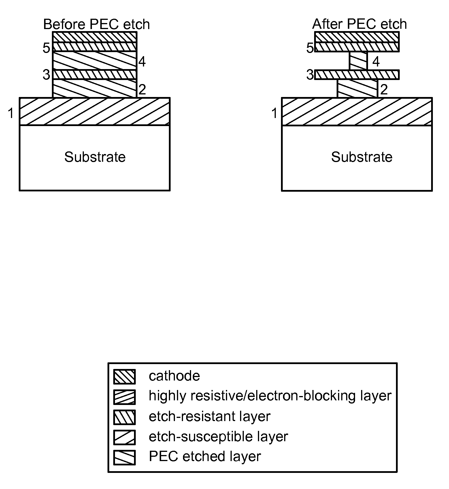
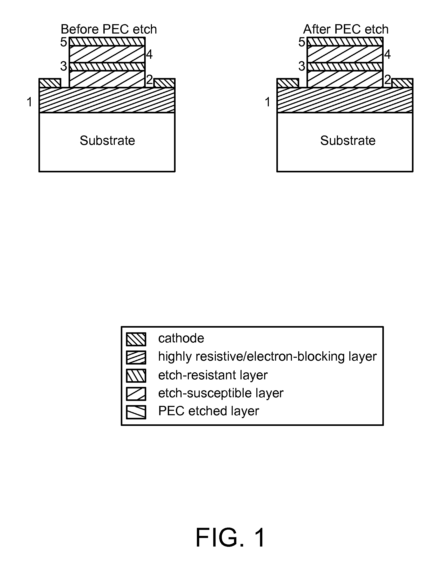
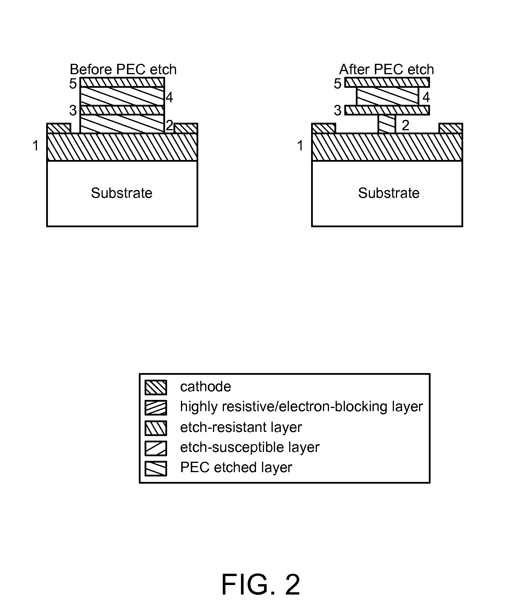
This patent describes a way to make semiconductor structures using a process called PEC etching. This process uses a laser or a broad-spectrum light source to generate electrons and holes in layers with lower energy than the incident light. The etching is controlled by modifying the electrical potential of the structure relative to the electrolyte and using layers that impede electron flow or a cathode to collect the photo-generated carriers. This invention can be used to make various semiconductor structures and techniques, such as substrate removal.

Problems solved by technology

In PEC etching of semiconductor multilayer structures, variability can arise from (a) non-uniform illumination of the sample (e.g. via absorption of the incident light), (b) geometry-dependent limitations to the availability of electrolyte (as would characterize the wetting of electrolyte between two very closely spaced layers of material), and (c) carrier diffusion and recombination dynamics that vary strongly with geometry and position of the carriers within a structure.
This invention also allows for significant improvements over existing practices in the following nitride-based applications:
1) Electrical and optical apertures in nitride-based electronic and optoelectronic devices: Currently used methods typically employ some form of ion implantation, which may cause unwanted damage to critical layers [11]; or dry etching followed by regrowth, which is an elaborate and cumbersome process [12]. In recent years, PEC etching has been used to create current apertures in electrical devices [1]; however, due to the lack of etch control, the material composition of the undercut layers is highly restricted. Thus, possible device designs for these geometries are limited.
2) Substrate removal and cavity thinning: Currently, the commonly used methods include laser-assisted debonding [13, 14] and inductively coupled plasma (ICP) etching [15-17] or polishing, respectively. These methods are cumbersome, and typically result in relatively imprecise material thicknesses.
3) Semiconductor membranes and cantilevers: Currently, PEC etching is used to create undercut structures such as membranes and cantilevers in the nitride material system [3, 5, 7, 18]; however, due to the lack of etch control, the material composition of the undercut layers is highly restricted [18]. Therefore, possible designs for undercut devices such as micro-electro-mechanical systems (MEMS) and photonic crystals are extremely limited.

Method used


Image

  • Control of photoelectrochemical (PEC) etching by modification of the local electrochemical potential of the semiconductor structure relative to the electrolyte
  • Control of photoelectrochemical (PEC) etching by modification of the local electrochemical potential of the semiconductor structure relative to the electrolyte
  • Control of photoelectrochemical (PEC) etching by modification of the local electrochemical potential of the semiconductor structure relative to the electrolyte

Examples


Embodiment Construction

[0033]In the following description of the preferred embodiment, reference is made to the accompanying drawings which form a part hereof, and in which is shown by way of illustration a specific embodiment in which the invention may be practiced. It is to be understood that other embodiments may be utilized and structural changes may be made without departing from the scope of the present invention.

[0034]General Purpose

[0035]PEC etching is a viable method for producing specific geometries in the III-nitride material system, forming three-dimensional structures that would be extremely challenging to produce with gas-phase etching processes or more standard wet chemical etching. The existence of a controlled three-dimensional etch process can give rise to numerous useful device geometries. Specifically, an undercut geometry is desirable in several applications including but not limited to microdisk resonators, air-gap DBRs, semiconductor membranes and cantilevers, electrical and optical...


PUM


Abstract

A method for locally controlling an electrical potential of a semiconductor structure or device, and hence locally controlling lateral and / or vertical photoelectrochemical (PEC) etch rates, by appropriate placement of electrically resistive layers or layers that impede electron flow within the semiconductor structure, and / or by positioning a cathode in contact with specific layers of the semiconductor structure during PEC etching.

Description

CROSS-REFERENCE TO RELATED APPLICATIONS[0001]This application claims the benefit under 35 U.S.C. Section 119(e) of the following co-pending and commonly-assigned U.S. patent application:[0002]U.S. Provisional Patent Application Ser. No. 60 / 624,308, filed on Nov. 2, 2004, by Evelyn L. Hu, Shuji Nakamura, Elaine D. Haberer, and Rajat Sharma, entitled “CONTROL OF PHOTOELECTROCHEMICAL (PEC) ETCHING BY MODIFICATION OF THE LOCAL ELECTROCHEMICAL POTENTIAL OF THE SEMICONDUCTOR STRUCTURE RELATIVE TO THE ELECTROLYTE”;[0003]which application is incorporated by reference herein.BACKGROUND OF THE INVENTION[0004]1. Field of the Invention[0005]The present invention relates to the control of photoelectrochemical (PEC) etching by modification of the local electrochemical potential of the semiconductor structure relative to the electrolyte.[0006]2. Description of the Related Art[0007](Note: This application references to various publications as indicated in the specification by reference numbers encl...

Claims


Application Information

Patent Timeline
Patent Type & Authority Patents(United States)
IPC IPC(8): H01L21/302H01L21/461H01L33/10
CPCB82Y20/00H01L21/30635H01S5/1075H01L33/10H01S5/18316H01S5/2081H01S5/34333H01S2304/12
Inventor HU, EVELYN L.NAKAMURA, SHUJIHABERER, ELAINE D.SHARMA, RAJAT
Owner RGT UNIV OF CALIFORNIA
Learn More