

Semiconductor device having junction termination extension
a semiconductor device and junction technology, applied in the direction of pulse generators, pulse techniques, instruments, etc., can solve the problems of inability to obtain a breakdown voltage close to an ideal breakdown voltage, many difficulties in the field of semiconductor device structure, and manufacturing costs, so as to achieve sufficient breakdown voltage characteristics, suppress the occurrence of electric field concentration, and form easily
- Summary
- Abstract
- Description
- Claims
- Application Information
AI Technical Summary
Benefits of technology
Problems solved by technology
Method used
Image

Examples
first preferred embodiment
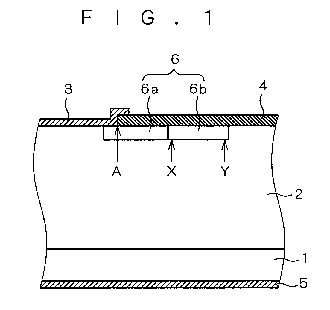
[0022]FIG. 1 is a sectional view showing the structure of a semiconductor device according to a first preferred embodiment of the present invention. The semiconductor device is provided with a Schottky barrier diode formed on an SiC substrate 1. More specifically, an n-type SiC drift layer 2 is formed in the n-type SiC substrate 1, and an anode electrode 3 (Schottky electrode) is formed on the upper surface of the SiC drift layer 2 to come into Schottky contact with the drift layer 2. The drift layer 2 is set to have an impurity concentration (doping) of 2×10¹⁵ to 12×1015 cm−3 and a thickness of 5 to 15 μm such that the diode can achieve a breakdown voltage of about 1000 V. An insulating film 4 is also formed on the upper surface of the drift layer 2 in a region which does not come into contact with the anode electrode 3. A cathode electrode 5 of the diode is provided on the bottom of the SiC substrate 1.
[0023]A JTE region 6 is formed as an edge termination outside the anode electro...
second preferred embodiment
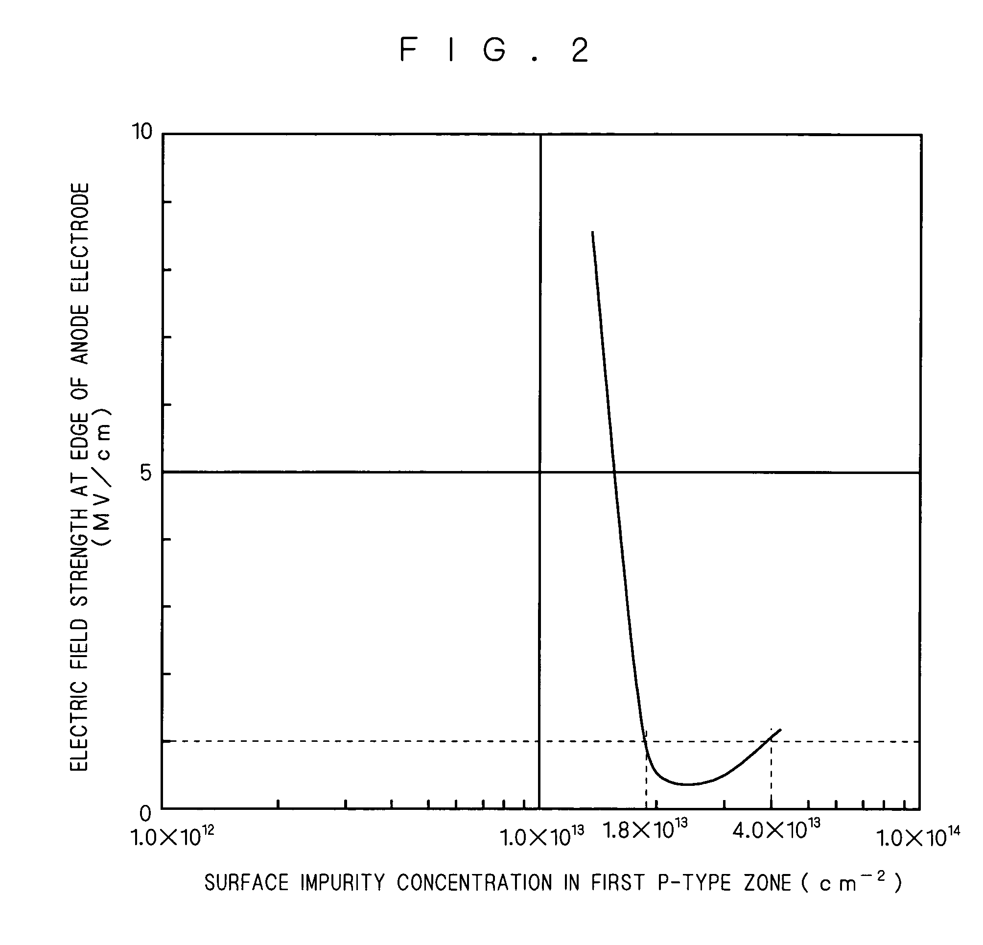
[0035]In the first preferred embodiment, the first and second p-type zones 6a and 6b are formed in the same thickness as shown in FIG. 1. Then, the surface impurity concentration of the first p-type zone 6a is set at 1.8×10¹³ to 4×1013 cm−2 and that of the second p-type zone 6b is set at 1×10¹³ to 2.5×1013 cm−2 by adjusting the impurity concentration of respective zones.
[0036]As described earlier, however, the surface impurity concentration is obtained by multiplying the impurity concentration of an impurity region by the thickness of the impurity region. Accordingly, the surface impurity concentration can also be adjusted by adjusting the thickness of the impurity region.
[0037]FIG. 4 is a sectional view showing the structure of a semiconductor device according to a second preferred embodiment of the invention. In this drawing, components similar to those shown in FIG. 1 are indicated by the same reference characters, and detailed description thereof is thus omitted here.
[0038]In th...
third preferred embodiment
[0041]In the conventional JTE, as described earlier, the electric field concentration occurs at the border between a plurality of p-type zones making up the JTE region, i.e., a position in which the charge level abruptly changes in the JTE region. In the present embodiment, a JTE capable of suppressing the occurrence of electric field concentration in a JTE region will be described.
[0042]FIG. 5 is a sectional view showing the structure of a semiconductor device according to a third preferred embodiment of the invention. In this drawing, components similar to those shown in FIG. 1 are indicated by the same reference characters.
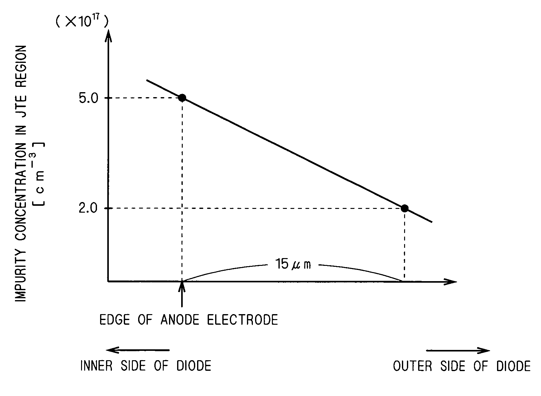
[0043]The p-type zones making up the JTE region 6 are formed to extend under the edge of the anode electrode 3 and to reach 20 μm or more outwardly away from the edge. In the present embodiment, the JTE region 6 has a constant thickness as shown in FIG. 5, and a continuously decreasing impurity concentration outwardly from the edge of the anode electrode 3. In ...
PUM
 Abstract
Description
Claims
Application Information