
Method for forming perovskite type oxide thin film, piezoelectric element, liquid discharge head, and liquid discharge apparatus

a technology of piezoelectric elements and thin films, applied in the direction of basic electric elements, printing, generators/motors, etc., can solve the problems of inability to develop a micro-electromechanical system to a minute device, inability to obtain a long ink-jet head, and limited size, etc., to achieve high conductivity, high conductivity, and preferable adhesiveness

Inactive Publication Date: 2009-07-28
CANON KK
View PDF9 Cites 4 Cited by
  • Summary
  • Abstract
  • Description
  • Claims
  • Application Information

AI Technical Summary

Benefits of technology

The present invention provides a new method for forming a perovskite type oxide thin film with multiple elements in a preferred crystal structure. This method can be used for various dielectric devices and can produce high-quality thin films with good crystallinity and orientation. The method can also be used to form a piezoelectric substance with large piezoelectricity and a liquid discharge head with uniform and high performance. The invention also provides a liquid discharge apparatus with the liquid discharge head.

Problems solved by technology

Therefore, it is necessary to cut, work, and join a single crystal material to form it into a device and its size is limited.
For example, there are problems that it is impossible to develop a micromachine (MEMS; Micro Electro Mechanical System) to a minute device or it is impossible to obtain a long ink-jet head.
Furthermore, it is conventionally difficult to form a relaxor state of single crystal known as zinc niobate titanate (may be shown as PZN—PT) in the case of the sputtering method or sol-gel method.
Moreover, it is difficult to work a single crystal material because it has an insufficient mechanical strength and its workability is not preferable as a target.
In the case of the sol-gel method or metal organic-compound deposition method (may be shown as MOD method), there are problems that it is difficult that the organic-metal compound of Zn which is a material is melted in a solvent when it is coexistent with other material and it is impossible to form a composition in which the content of Zn element is increased into a film.

Method used


Image

  • Method for forming perovskite type oxide thin film, piezoelectric element, liquid discharge head, and liquid discharge apparatus
  • Method for forming perovskite type oxide thin film, piezoelectric element, liquid discharge head, and liquid discharge apparatus
  • Method for forming perovskite type oxide thin film, piezoelectric element, liquid discharge head, and liquid discharge apparatus

Examples


example 1

[0116]A PZN—PT thin film which is a perovskite type oxide thin film is formed by using the MO-CVD method.

[0117][Material]

[0118]Pb(thd)2 is used as a Pb material, Zn(EDMDD)2 is used as a Zn material, (C2H5)5Nb is used as a Nb material and Ti(i-C3H7O)4 is used as a Ti material.

[0119][Fabrication Method]

[0120]A substrate in which a SRO(100) electrode is formed on a STO(100) substrate is used. The introduction quantity of a source gas is adjusted while adjusting the temperature of the substrate to 600° C. and partial pressures of oxygen gas and nitrogen gas to 330 Pa.

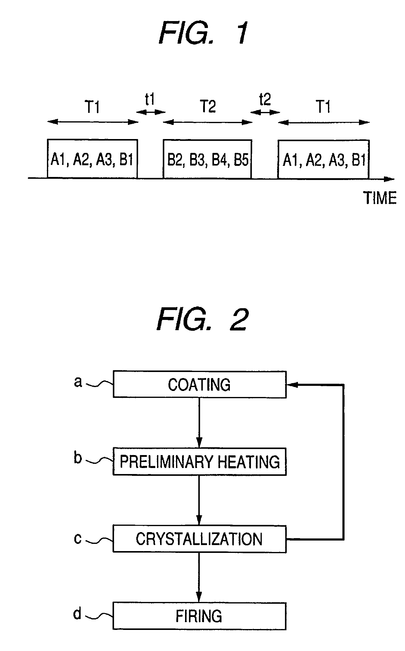
[0121]Because A-site element is Pb and B-site elements are Zn, Nb and Ti, they are grouped into group I(Pb and Ti) and group II(Zn and Nb) and each material containing elements included in the groups is supplied onto the substrate in separate steps.

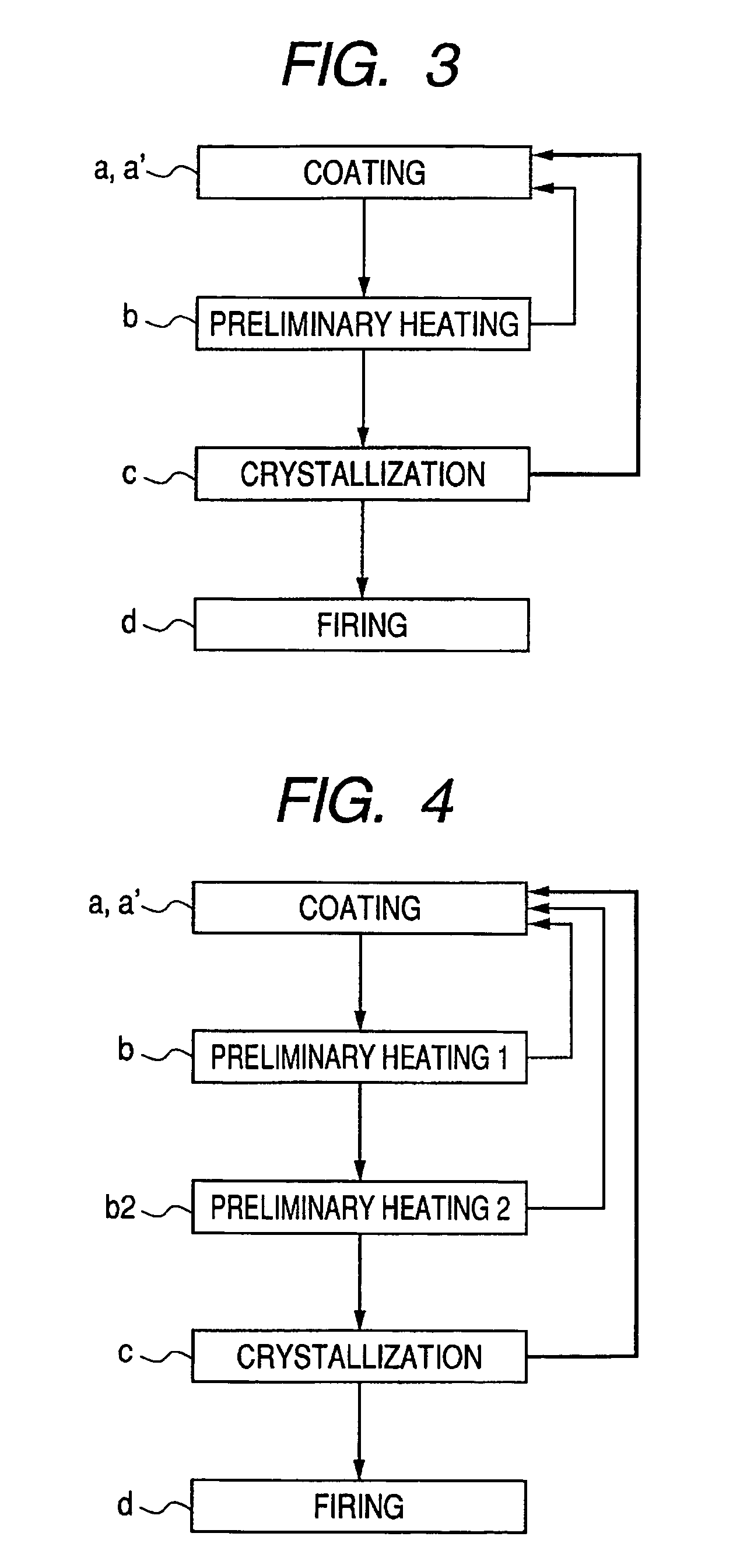
[0122]First, a first step for supplying Pb and Ti for 10 sec is performed. Then, supply of the materials is stopped for 5 sec to calcinate a thin film formed on the substrate at ...

example 2

[0124]A PZN—PT thin film (thickness of 0.89PZN-0.11PT is 1.5 μm) is obtained similarly to the case of the example 1 except that a substrate in which SRO(100) / LaNiO3(100) / CeO2(100) / YSZ(100) is laminated on Si(100) substrate is used. As a result of analyzing XRD and evaluating a piezoelectric characteristic similarly to the case of the example 1, the above thin film has a perovskite structure and a single crystal film having crystallinity of (100) is obtained. As a result of forming an upper electrode of 100 μmφ and measuring d33, a preferable piezoelectric characteristic of 350 pm / V is shown.

example 3

[0125]A PZN—PT film is formed by the method same as the case of the example 1 on an SOI substrate in which SOI layer has a thickness of 3 μm and a box layer has a thickness of 0.5 μm through an SRO(100) electrode. Because in the case of this substrate, a box layer functions as an etching stop layer, it is advantageous for working in subsequent steps and it is possible to obtain an element having preferable adhesiveness when using an SOI layer as a vibration plate.

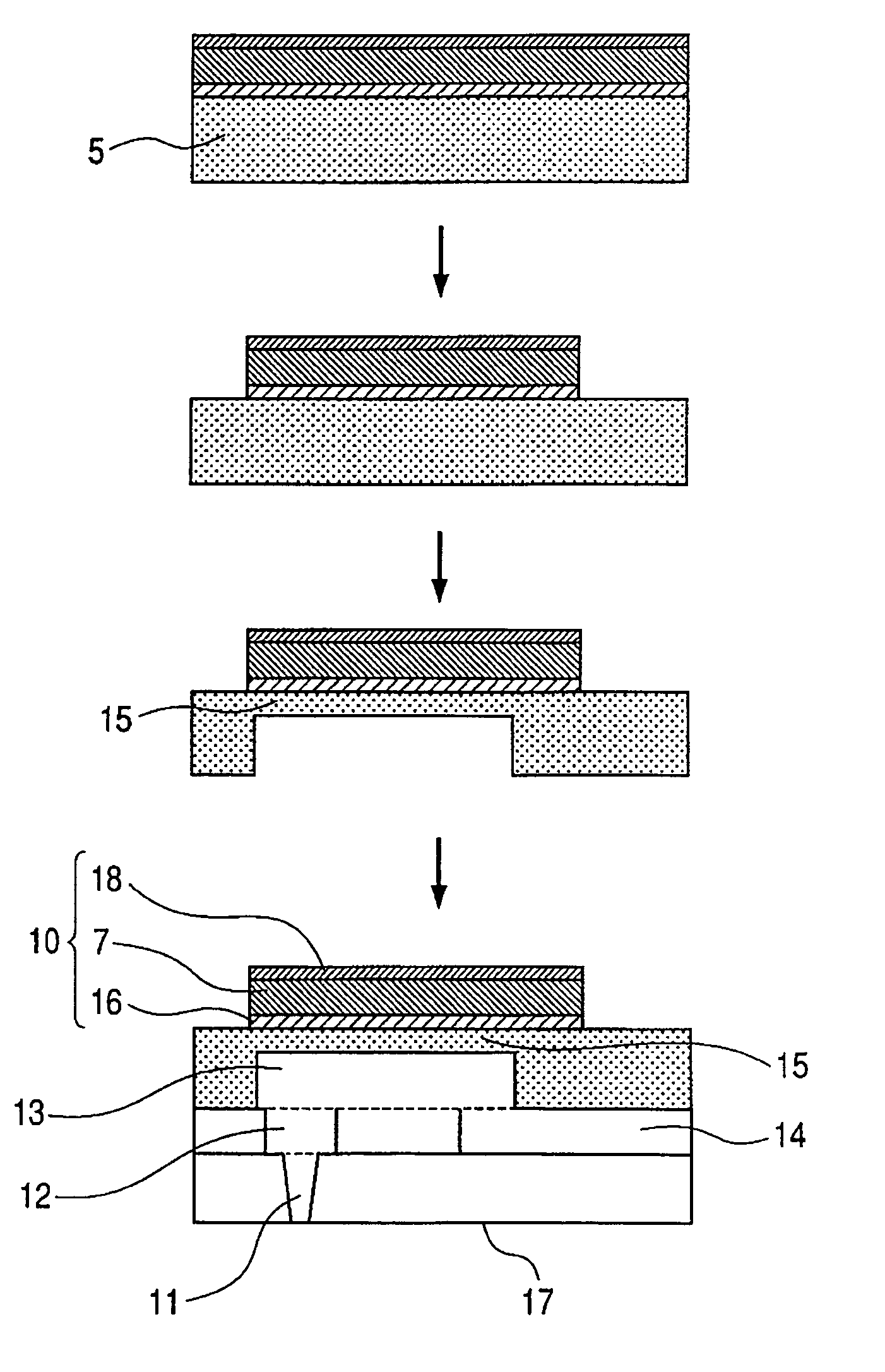
[0126]By etching the handle layer of an SOI substrate, a separate liquid chamber and liquid supply port are obtained. By joining the separate liquid chamber and liquid supply port with a substrate having a discharge port, the liquid discharge head shown in FIG. 6 is prepared. The separate liquid chamber is worked into a length of 100 μm and length of 3 mm. A voltage of 30 V is applied to a PZN—PT layer which is a piezoelectric element at 25 kHz to measure the displacement of an SOI layer serving as a vibration plate. It is ...


PUM

PropertyMeasurementUnit
thicknessaaaaaaaaaa
thicknessaaaaaaaaaa
thicknessaaaaaaaaaa

Abstract

To provide a film forming method capable of obtaining a high-quality perovskite type oxide thin film, piezoelectric element having a piezoelectric substance constituted of the thin film formed by the film forming method, liquid discharge head having the piezoelectric element and liquid discharge apparatus having the liquid discharge head. A method for forming a perovskite type oxide thin film having a composition expressed by (A1x, A2y A3z) (B1j, B2k, B3l, B4m B5n)Op is included, which is a film forming method having a plurality of steps for supplying a material containing the elements onto the substrate, dividing the elements A1 to A3 and B1 to B5 into a plurality of groups and supplying each material containing the elements included in the groups onto the substrate in separate steps.

Description

BACKGROUND OF THE INVENTION[0001]1. Field of the Invention[0002]The present invention relates to a method for forming a perovskite type oxide thin film having a plurality of A-site elements or B-site elements, piezoelectric element having a piezoelectric substance constituted of a perovskite type oxide thin film formed by the film forming method, liquid discharge head having the piezoelectric element, and liquid discharge apparatus having the liquid discharge head.[0003]2. Description of the Related Art[0004]Recently, researches of a ferroelectric thin film and piezoelectric electrostriction thin film are frequently performed as application to an FeRAM, application to an optical shutter and optical communication, and application to a piezoelectric actuator. In this case, as a material having a large piezoelectric characteristic, a relaxor state of single crystal material is reported. It is said that the relaxor state of single crystal material shows a large piezoelectric characteris...

Claims


Application Information

Patent Timeline
Patent Type & Authority Patents(United States)
IPC IPC(8): H01L41/00H01L41/187H10N30/853
CPCB41J2/14233B41J2/161B41J2/1623B41J2/1628B41J2/1629B41J2/1631B41J2/1634B41J2/1642B41J2/1646H01L41/1875H01L41/316H01L41/318B41J2/1632H01L41/0973H10N30/2047H10N30/8548H10N30/076H10N30/078
Inventor FUKUI, TETSUROTAKEDA, KENICHIMATSUDA, TAKANORIFUNAKUBO, HIROSHIYOKOYAMA, SHINTARO
Owner CANON KK
Learn More