Voltage controlled oscillator, and PLL circuit and wireless communication apparatus using the same

a technology of voltage control and oscillator, which is applied in the direction of pulse generator, pulse technique, modulation, etc., can solve the problems of difficult to use variable capacitance elements having a high level of linearity, difficult to achieve high-level linearity use of variable capacitance elements, and significant change in transient response characteristic and noise band characteristic in accordance with frequency, so as to increase the linearity of the change ratio of the oscillation frequency

Inactive Publication Date: 2009-07-28
PANASONIC CORP
View PDF4 Cites 6 Cited by
  • Summary
  • Abstract
  • Description
  • Claims
  • Application Information

AI Technical Summary

Benefits of technology

[0015]Therefore, an object of the present invention is to provide a voltage controlled oscillator for allowing a capacitance value to be changed gradually over a wide range of control voltage without enlarging the chip area, so as to increase the linearity of the change ratio of the oscillation frequency with respect to the control voltage, and a PLL circuit and a wireless communication apparatus using such a voltage controlled oscillator.
[0017]One of the two terminals of the variable capacitance element is supplied with a control voltage for controlling an oscillation frequency, and the other terminal of the variable capacitance element is supplied with a reference voltage which is output from the time-switched level shift circuit. Alternatively, one of the two terminals of the variable capacitance element is supplied with a control voltage for controlling an oscillation frequency and a voltage which is output from the time-switched level shift circuit, and the other terminal of the variable capacitance element is supplied with a fixed reference voltage. In the latter case, it is possible to eliminate the capacitive element.
[0020]The present invention realizes a voltage controlled oscillator for allowing a capacitance value to be gradually changed over a wide range of control voltage without enlarging the chip area, so as to increase the linearity of the change ratio in the oscillation frequency with respect to the control voltage, and a PLL circuit and a wireless communication apparatus using such a voltage controlled oscillator.

Problems solved by technology

In an area where the frequency sensitivity with respect to the control voltage Vt is high, there is a problem that the frequency is changed even by slight noise applied to the frequency control terminal 607, and thus the phase noise characteristic is lowered.
In actuality, however, it is difficult to use variable capacitance elements having a high level of linearity as the variable capacitance elements 611 and 612 in the conventional voltage controlled oscillator 600 formed on a semiconductor substrate.
As a result, a PLL circuit including the conventional voltage controlled oscillator 600 has a problem that the transient response characteristic and the noise band characteristic significantly change in accordance with the frequency.
This involves a problem of enlarging the chip area.
In addition, since it is difficult to lay out a large number of variable capacitance circuits in parallel on a semiconductor substrate, there is a limit on the number of the variable capacitance circuits.
Thus, it is still difficult to allow the capacitance value to be changed gradually over a wide range of control voltage Vt.

Method used


Image

  • Voltage controlled oscillator, and PLL circuit and wireless communication apparatus using the same
  • Voltage controlled oscillator, and PLL circuit and wireless communication apparatus using the same
  • Voltage controlled oscillator, and PLL circuit and wireless communication apparatus using the same

Examples


first embodiment

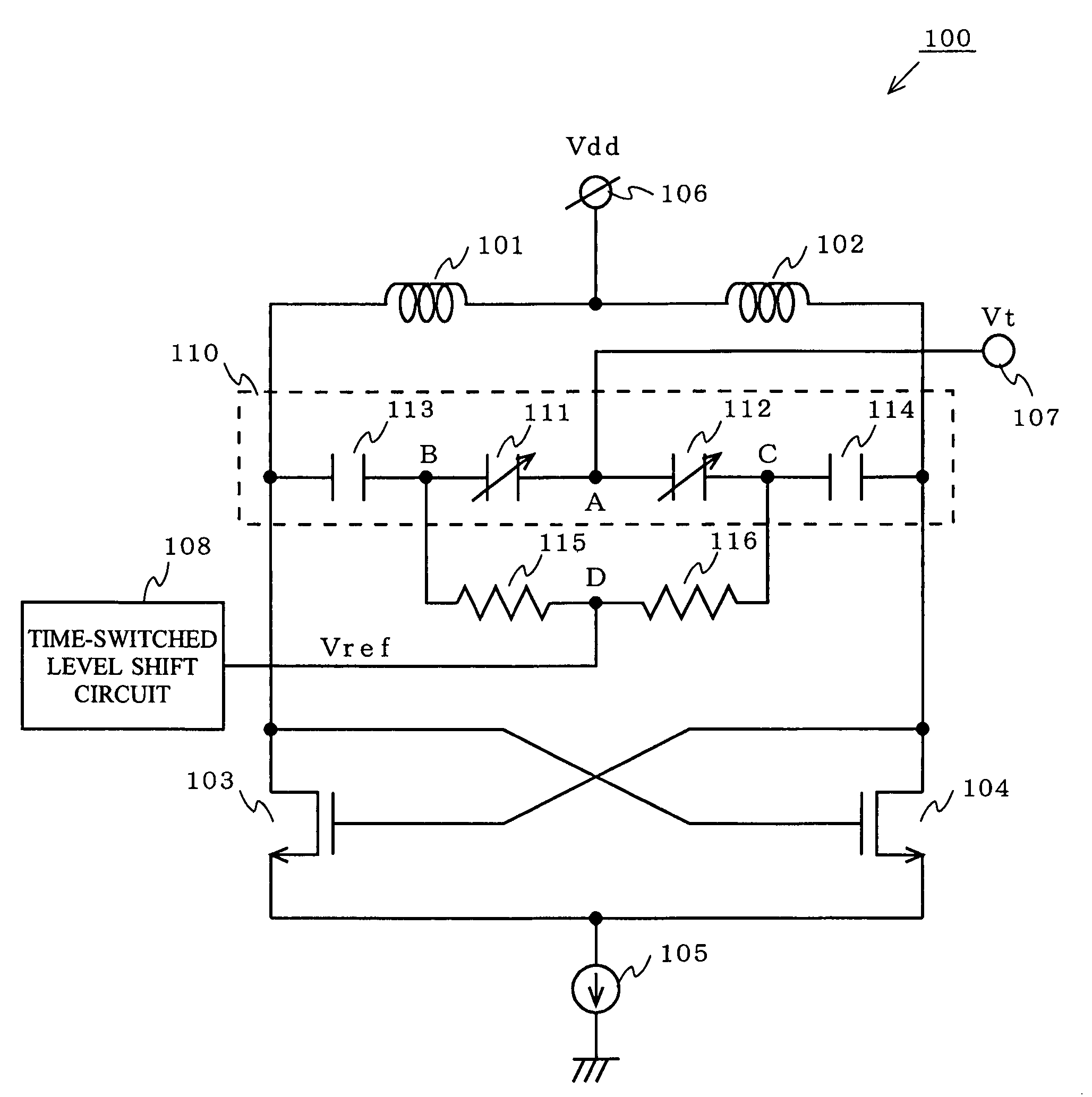
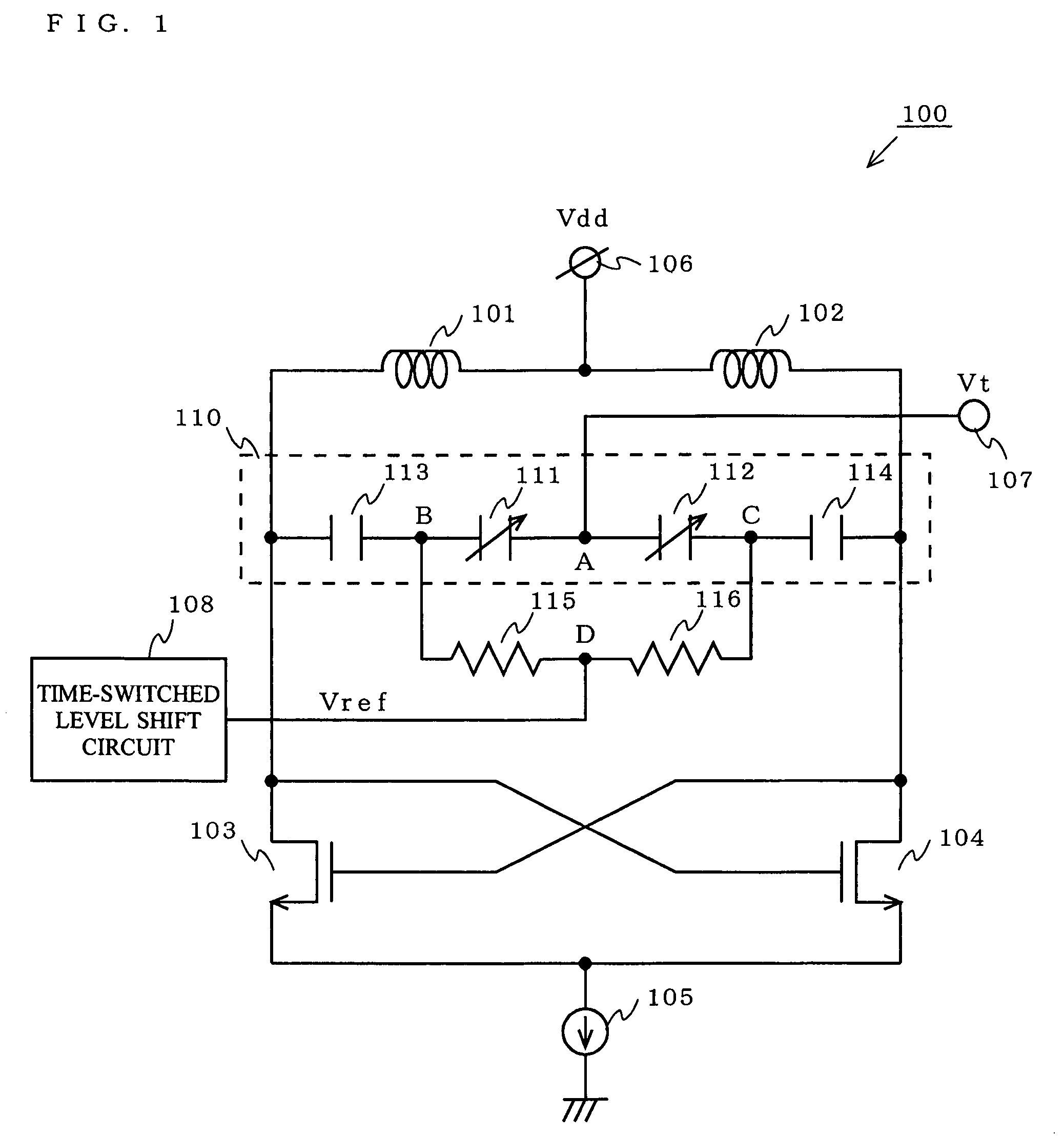
[0045]FIG. 1 shows a structure of a voltage controlled oscillator 100 according to a first embodiment of the present invention. As shown in FIG. 1, the voltage controlled oscillator 100 according to the first embodiment includes inductors 101 and 102, oscillating transistors 103 and 104, a current source 105, a time-switched level shift circuit 108, variable capacitance elements 111 and 112, DC cutting capacitive elements 113 and 114, and radio frequency inhibiting resistors 115 and 116.

[0046]The inductors 101 and 102 are connected to each other in series to form an inductor circuit. The oscillating transistors 103 and 104 are cross-coupled to each other to form a negative resistance circuit. As the oscillating transistors 103 and 104, MOS transistors or bipolar transistors are suitable. The variable capacitance elements 111 and 112 and the DC cutting capacitive elements 113 and 114 form a variable capacitance circuit 110 by the following connections. The variable capacitance elemen...

second embodiment

[0067]FIG. 9 shows a structure of a voltage controlled oscillator 210 according to a second embodiment of the present invention. As shown in FIG. 9, the voltage controlled oscillator 210 according to the second embodiment is different from the voltage controlled oscillator 100 according to the first embodiment in the position of the time-switched level shift circuit 108. The elements of the voltage controlled oscillator 210 are basically the same as those of the voltage controlled oscillator 100 described above in terms of the detailed circuit configuration and operation, and thus bear the identical reference numerals thereto and descriptions thereof will be omitted.

[0068]In the voltage controlled oscillator 210, the output terminal of the time-switched level shift circuit 108 is connected to the frequency control terminal 107. Owing to this structure, the output voltage value from the time-switched level shift circuit 108, which changes in accordance with time, is applied to the co...

third embodiment

[0072]FIG. 11 shows a structure of a voltage controlled oscillator 310 according to a third embodiment of the present invention. As shown in FIG. 11, the voltage controlled oscillator 310 according to the third embodiment includes inductors 101 and 102, oscillating transistors 103 and 104, a current source 105, a time-switched level shift circuit 108, and variable capacitance elements 111 and 112.

[0073]The voltage controlled oscillator 310 according to the third embodiment has a structure obtained by eliminating the DC cutting capacitive elements 113 and 114 and the radio frequency inhibiting resistors 115 and 116 from the voltage controlled oscillator 210 according to the second embodiment. The elements of the voltage controlled oscillator 310 are basically the same as those of the voltage controlled oscillators 100 and 210 described above in terms of the detailed circuit configuration and operation, and thus bear the identical reference numerals thereto and descriptions thereof wi...


PUM


Abstract

A voltage controlled oscillator including an inductor circuit including inductors 101, 102, a variable capacitance circuit 110 having variable capacitance elements 111, 112 changing a capacitance according to a voltage difference between two terminals thereof and having capacitive elements 113, 114 cutting a DC component, a negative resistance circuit including cross-coupled oscillating transistors 103, 104, and a time-switched level shift circuit 108 for shifting a reference voltage to two or more levels in a predetermined period. A connection point A of the variable capacitance elements is supplied with a control voltage Vt controlling an oscillation frequency, and connection points B, C of the variable capacitance elements and the capacitive elements are supplied with a reference voltage Vref output from the time-switched level shift circuit 108 via resistors 115, 116.

Description

BACKGROUND OF THE INVENTION[0001]1. Field of the Invention[0002]The present invention relates to a voltage controlled oscillator usable for, for example, generating a local oscillation signal of a wireless communication apparatus, and a PLL circuit and a wireless communication apparatus using the same.[0003]2. Description of the Background Art[0004]A voltage controlled oscillator (VCO) is widely used as a device for generating a local oscillation signal of a wireless communication apparatus. FIG. 15 shows an exemplary structure of a conventional voltage controlled oscillator 600. The conventional voltage controlled oscillator 600 includes inductors 601 and 602, variable capacitance elements 611 and 612, oscillating transistors 603 and 604, a current source 605 and a power supply terminal 606 that receives a voltage Vdd.[0005]The inductors 601 and 602 and the variable capacitance elements 611 and 612 form a parallel resonance circuit. A capacitance value of the variable capacitance e...

Claims


Application Information

Patent Timeline
Patent Type & Authority Patents(United States)
IPC IPC(8): H03B1/00
CPCH03J5/00H03L7/099H03B5/1293H03B5/1228H03B5/1215H03B5/1253H03B2200/005H03L2207/06
Inventor TSUKIZAWA, TAKAYUKI
Owner PANASONIC CORP
Why Eureka
Try Eureka