
Nonvolatile memory device using variable resistive element

a resistive element and memory device technology, applied in information storage, static storage, digital storage, etc., can solve the problems of operation errors during read operations, reducing sensing margins, and affecting the reliability of read operations, so as to reduce noise, improve read operation reliability, and increase sensing margins

Active Publication Date: 2009-08-04
SAMSUNG ELECTRONICS CO LTD
View PDF10 Cites 8 Cited by
  • Summary
  • Abstract
  • Description
  • Claims
  • Application Information

AI Technical Summary

Benefits of technology

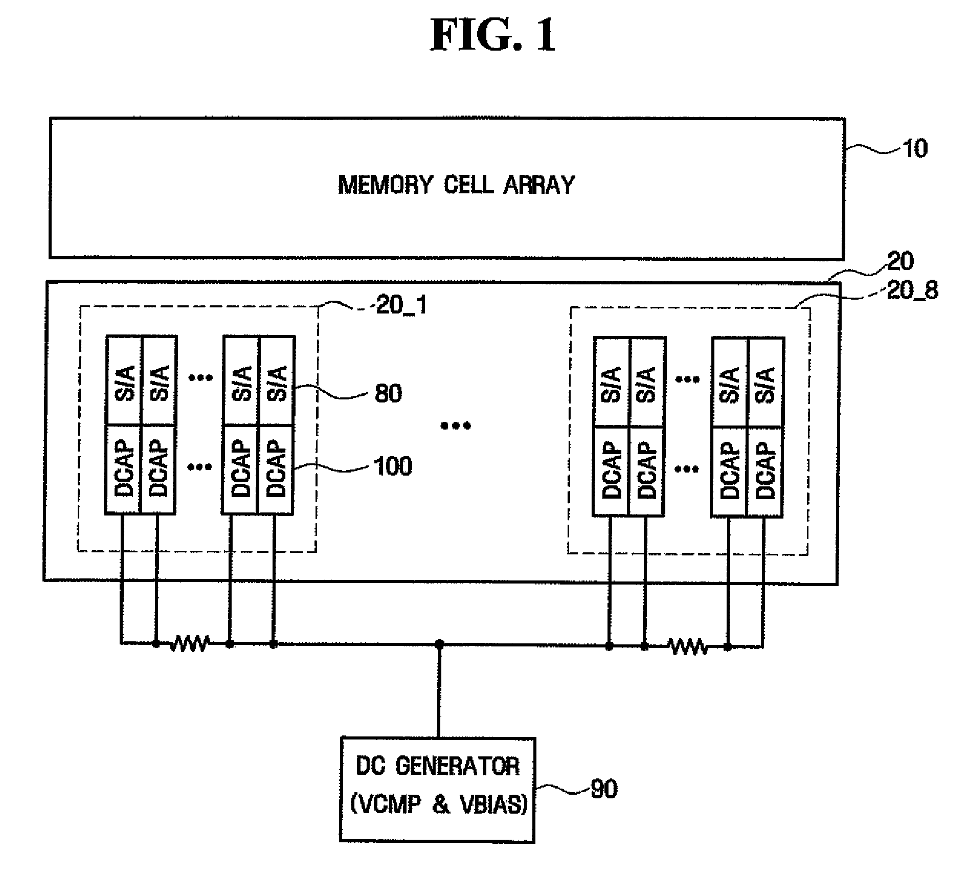
The invention provides a nonvolatile memory device and a data read circuit that use a variable resistive element. The data read circuit includes a clamping unit, a precharge unit, a read bias supply unit, a sense amplifier, and a first decoupling unit. The first decoupling unit reduces noise in the clamping control signal or the read bias control signal. This improves the sensing margin and reliability of read operations in memory devices with variable resistive elements.

Problems solved by technology

This reduces a sensing margin, and thus, it may be impossible for the sense amplifier to accurately differentiate a set state from a reset state.
That is, an operation error may occur during the read operation.

Method used


Image

  • Nonvolatile memory device using variable resistive element
  • Nonvolatile memory device using variable resistive element
  • Nonvolatile memory device using variable resistive element

Examples


first embodiment

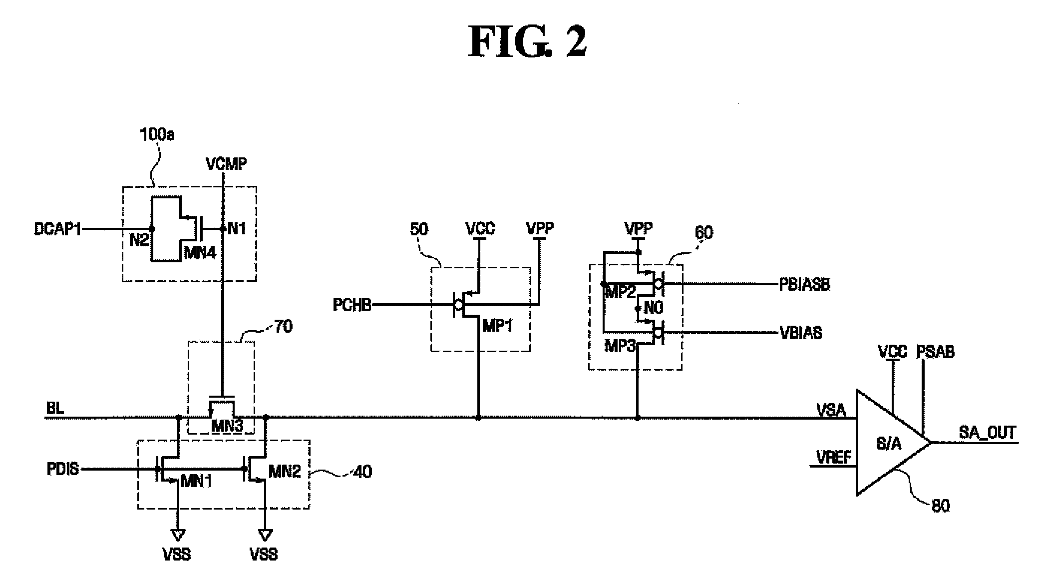
[0039]FIG. 2 is a circuit diagram illustrating a data read circuit that is used in a nonvolatile memory device according to the present invention. FIG. 3 is a timing diagram illustrating the operation of the data read circuit shown in FIG. 2. FIG. 4 is a circuit diagram of a portion of the data read circuit shown in FIG. 2.

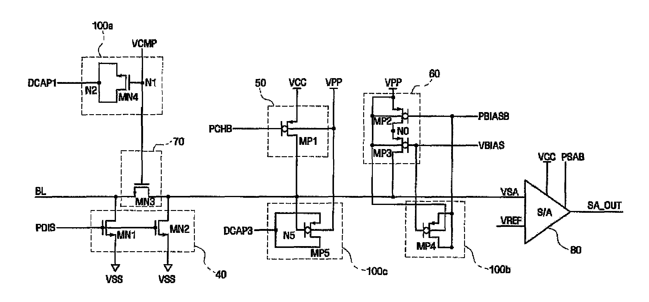
[0040]First, referring to FIG. 2, the data read circuit that is used in the nonvolatile memory device according to the first embodiment of the present invention includes a discharge unit 40, a precharge unit 50, a read bias supply unit 60, a clamping unit 70, a sense amplifier 80, and a decoupling unit 100a.

[0041]The discharge unit 40 discharges a sensing node VSA and / or a bit line BL coupled to a nonvolatile memory cell that is selected before the data read operation, with a predetermined level, for example, with a ground voltage VSS. The discharge unit 40 may include an NMOS transistor MN1 that is coupled between the bit line BL and the ground voltage terminal ...

second embodiment

[0058]FIG. 5 is a circuit diagram illustrating a data read circuit that is used in a nonvolatile memory device according to the present invention. FIG. 6 is a timing diagram illustrating the operation of the data read circuit shown in FIG. 5. FIG. 7 is a circuit diagram of a portion of the data read circuit shown in FIG. 5. The same components as those in FIGS. 2 to 4 are denoted by the same reference numerals, and the detailed description thereof will be omitted. The embodiment of FIG. 5 does not include the decoupling unit 100a.

[0059]Referring to FIG. 5, a decoupling unit 100b that is used in the nonvolatile memory device according to a second embodiment of the present invention removes noise of a read bias control signal VBIAS. Specifically, when a read bias supply unit 60 starts to supply a read bias to a sensing node VSA, it is possible to remove the noise that affects the read bias control signal VBIAS. The decoupling unit 100b may include a second decoupling capacitor MP4 th...

third embodiment

[0069]FIG. 8 is a circuit diagram illustrating a data read circuit that is used in a nonvolatile memory device according to the present invention. The same components as those in FIGS. 2 to 7 are denoted by the same reference numerals, and the detailed description thereof will be omitted.

[0070]Referring to FIG. 8, the nonvolatile memory device according to the third embodiment of the present invention includes both the decoupling unit 100a described in FIG. 2 and the decoupling unit 100b described in FIG. 5. The nonvolatile memory device according to the third embodiment of the present invention removes noise of a clamping control signal VCMP and noise of a read bias control signal VBIAS. Therefore, it is possible to increase a sensing margin and improve reliability of a read operation.


PUM


Abstract

Disclosed is a nonvolatile memory device using a variable resistive element, and a data read circuit for use in variable resistive memory devices. More specifically, embodiments of the invention provide a data read circuit with one or more decoupling units to remove noise from one or more corresponding control signals. For instance, embodiments of the invention remove noise from a clamping control signal, a read bias control signal, and / or precharge signal. The disclosed decoupling units may be used alone or in any combination. Embodiments of the invention are beneficial because they can increase sensing margin and improve the reliability of read operations in memory devices with variable resistive elements.

Description

CROSS REFERENCE TO RELATED APPLICATION[0001]This application claims priority from Korean Patent Application No. 10-2007-0028202 filed on Mar. 22, 2007 in the Korean Intellectual Property Office, the disclosure of which is incorporated herein by reference in its entirety.BACKGROUND OF THE INVENTION[0002]1. Field of the Invention[0003]The present invention relates to a phase change memory device, and more particularly, to a phase change memory device that has improved reliability in a read operation.[0004]2. Description of the Related Art[0005]Examples of a nonvolatile memory device that uses a resistance material include a phase change random access memory (PRAM), a resistive random access memory (RRAM), a magnetic RAM (MRAM), and the like. A dynamic RAM (DRAM) device or a flash memory device stores data by using an electric charge, while a nonvolatile memory device that uses a resistance material stores data by using a change in state of a phase change material (PRAM), such as a cha...

Claims


Application Information

Patent Timeline
Patent Type & Authority Patents(United States)
IPC IPC(8): G11C7/02
CPCG11C13/00G11C13/0004G11C13/0061G11C13/004G11C2013/0054G11C7/02G11C2013/0045
Inventor CHOI, BYUNG-GILKIM, DU-EUNG
Owner SAMSUNG ELECTRONICS CO LTD
Learn More