Clock data recovery loop with separate proportional path

a proportional path and clock data technology, applied in the field of clock data recovery loops with separate proportional paths, can solve the problems of degrading loop stability, difficult loop design, and difficult to increase the capacitance in an on-chip solution, and achieve the effect of increasing stability in the bang-bang cdr loop

Inactive Publication Date: 2009-08-25
ALTERA CORP
View PDF8 Cites 36 Cited by
  • Summary
  • Abstract
  • Description
  • Claims
  • Application Information

AI Technical Summary

Benefits of technology

[0006]The present invention increases stability in a Bang-Bang CDR loop by providing alternate paths in the loop to be used in different frequency or data rate ranges. At relatively low frequencies or data rates, where the effect of the parasitic capacitance is small, the loop operates in a conventional manner, preferably with an RC loop filter. The effect of any parasitic or other capacitance that is in parallel with the loop filter is negligible. Thus, the loop operates as a well-understood, stable second-order loop, with the loop filter resistor R serving as a “proportional path” and the loop filter capacitor C serving as an “integral path.”
[0007]At higher frequencies or data rates, the effect of the parasitic or other capacitance is more significant, and gives rise to third-order effects which degrade loop stability and make loop design difficult. The effect can be reduced, and stability enhanced, by increasing the capacitance in the loop filter, making the parasitic or other capacitance less significant. However, while off-chip solutions (using an off-chip capacitor, which can be as large as necessary, in the loop filter) are available, increasing the capacitance is difficult in an on-chip solution, because of the device area requirements of a larger capacitor.
[0008]This invention provides an on-chip solution for a CDR circuit capable of operating in a stable, second-order mode over a wide range of data rates by introducing a separate proportional path at higher data rates. Thus, at lower data rates, the circuit operates conventionally as described above. At higher data rates, the resistor in the RC loop filter may be bypassed. This has the effect of creating a single capacitance (the parallel combination of the actual capacitor of the RC loop filter and the parasitic capacitance), returning the loop to a second-order condition. Because the resistor served as the proportional path as described above, when the resistor is bypassed, the Bang-Bang signal output of the Bang-Bang phase detector also is input directly to the signal generator (e.g., a voltage-controlled oscillator) of the loop circuit over a separate proportional path, bypassing the charge pump and loop filter. A varactor, which preferably is sized to generate a small frequency step (as discussed in more detail below), may be provided at that input, and receives the Bang-Bang signal output. This allows the output of the Bang-Bang phase detector to control the signal generator.

Problems solved by technology

At higher frequencies or data rates, the effect of the parasitic or other capacitance is more significant, and gives rise to third-order effects which degrade loop stability and make loop design difficult.
However, while off-chip solutions (using an off-chip capacitor, which can be as large as necessary, in the loop filter) are available, increasing the capacitance is difficult in an on-chip solution, because of the device area requirements of a larger capacitor.

Method used


Image

  • Clock data recovery loop with separate proportional path
  • Clock data recovery loop with separate proportional path
  • Clock data recovery loop with separate proportional path

Examples


exemplary embodiment 40

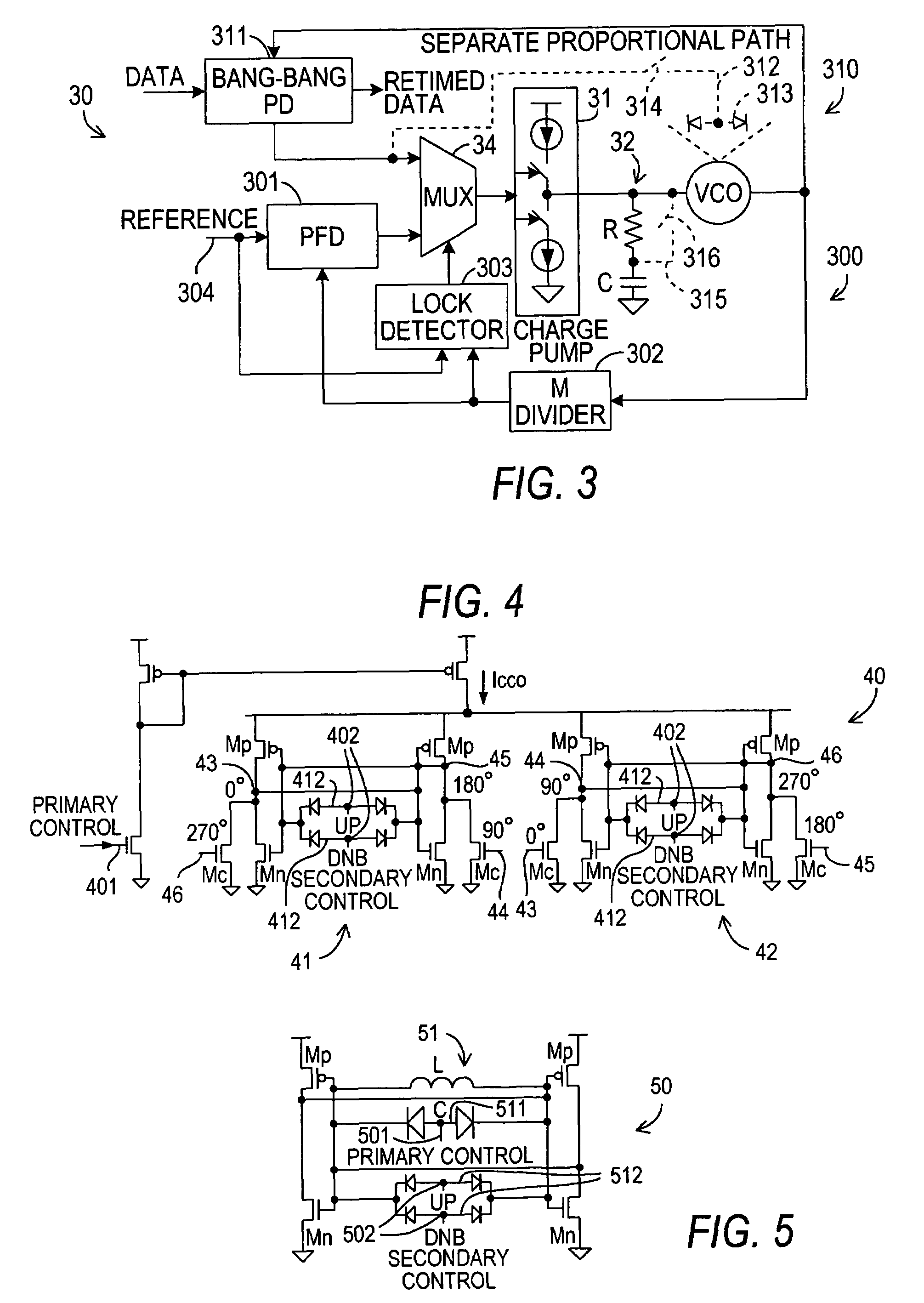
[0030]FIG. 4 shows a first exemplary embodiment 40 of a VCO 33 that can be used in loop circuits according to the present invention. VCO 40 preferably is a quadrature ring VCO preferably having two identical cross-coupled delay stages 41, 42. VCO 40 preferably provides quadrature phase clocks 43-46, and therefore preferably is suitable for half-rate Bang-Bang CDR applications.

[0031]VCO 40 preferably has two control inputs 401, 402. Control 401 preferably is the primary control, which preferably comes from loop filter 32. Control 402 preferably is the secondary control, which preferably comes from the Bang-Bang proportional path. Primary control 401 preferably determines the VCO tuning range while secondary control 402 (preferably including separate up and down signals UP and DNB) preferably determines the Bang-Bang step frequency fbb. Because fbb is on the order of 0.1% of the VCO center frequency as discussed above, the size of varactors 412 of secondary control 402 need be only la...

exemplary embodiment 50

[0032]FIG. 5 shows a second exemplary embodiment 50 of a VCO 33 that can be used in loop circuits according to the present invention. VCO 50 preferably is based on LC tank 51 with a larger varactor 511 proving the primary control 501 and smaller varactors 512 proving the secondary control 502. As shown, VCO 50 is designed for full-rate CDR operation. However, a quadrature LC VCO (not shown) for half-rate operation can be configured as two cross-coupled stages in a manner similar to that used in quadrature ring VCO 40.

[0033]A programmable logic device (“PLD”) 60 incorporating clock data recovery circuitry according to the present invention may be used in many kinds of electronic devices. One possible use is in a data processing system 900 shown in FIG. 6. Data processing system 900 may include one or more of the following components: a processor 901; memory 902; I / O circuitry 903; and peripheral devices 904. These components are coupled together by a system bus 905 and are populated ...


PUM


Abstract

A clock data recovery loop that can be used over a wide range of data rates and maintain second-order behavior includes a nonlinear (e.g., Bang-Bang) phase detector, a charge pump, an RC loop filter, and signal generator (e.g., a voltage controlled oscillator (VCO)). At low data rates, the loop may be operated with the charge pump and loop filter with stable second-order behavior, with the resistor R of the loop filter serving as a proportional path. A separate proportional path is also provided that provides phase detector output directly to a control input of the VCO, while the resistor R of the loop filter is also bypassed. As increasing data rates give rise to third-order effects, the separate proportional path may be activated to maintain second-order behavior.

Description

BACKGROUND OF THE INVENTION[0001]This invention relates to clock data recovery (CDR) applications. More particularly, this invention relates to a Bang-Bang CDR loop with a separate proportional path to improve loop stability.[0002]It is almost axiomatic that digital systems are clocked. When sampling data in a digital system, it is important to have an accurate clock, so that the sampling can occur as close as possible to the center of the data eye for accurate reading of the data. This is relatively easy when the clock is sent along with the data. However, when the clock must be recovered from the data, clock recovery errors could make centering the sampling time in the data eye difficult or unreliable. Any such problems are compounded in a programmable logic device, where the circuit paths, as well as the clock recovery circuitry, differ from one user logic design to the next.[0003]Clock recovery is commonly accomplished using a loop circuit—i.e., a phase-locked loop (PLL) or dela...

Claims


Application Information

Patent Timeline
Patent Type & Authority Patents(United States)
IPC IPC(8): H03D3/24
CPCH03K3/354H03L7/087H03L7/0891H03L7/093H03B5/1243H03L7/113H03L7/14H03L7/18H03B5/1228H03B5/1212H03L7/095H03L7/099H03L7/0995H04L7/0004H04L7/033
Inventor WANG, SHOUJUNMEI, HAITAOBEREZA, BILLKWASNIEWSKI, TAD
Owner ALTERA CORP
Why Eureka
Try Eureka