MEMS vibrating structure using a single-crystal piezoelectric thin film layer

a microelectromechanical system and thin film technology, applied in piezoelectric/electrostrictive/magnetostrictive devices, impedence networks, piezoelectric/electrostriction/magnetostriction machines, etc., can solve the problems of high loss, difficult control, limiting or expensive, etc., and achieve high accuracy

Active Publication Date: 2009-09-08
QORVO US INC
View PDF8 Cites 67 Cited by
  • Summary
  • Abstract
  • Description
  • Claims
  • Application Information

AI Technical Summary

Benefits of technology

[0007]The present invention relates to a micro-electro-mechanical systems (MEMS) vibrating structure having dominant lateral vibrations supported by a MEMS anchor system, and includes a single-crystal piezoelectric thin-film layer that has been grown with a specific crystal orientation, or wafer cut. Since the MEMS vibrating structure has dominant lateral vibrations, its resonant frequency may be controlled by its size and shape, rather than layer thickness, which provides high accuracy and enables multiple resonators having different resonant frequencies on a single substrate.
[0008]Since the MEMS vibrating structure is formed from a single-crystal material and uses mechanically efficient MEMS construction, it may be high-Q, low loss, stable, have a low temperature coefficient of frequency, have high repeatability, and have a low motional impedance.

Problems solved by technology

Therefore, a resonant frequency of the FBAR may be dependent upon the thickness of a deposited Aluminum Nitride layer, which may be difficult to control.
Additionally, a separate Aluminum Nitride layer may be needed for an additional FBAR having a different resonant frequency, which may be limiting or expensive.
However, the deposited thin-film of the FPOSR may have resonant frequency inaccuracies and may have high losses.

Method used


Image

  • MEMS vibrating structure using a single-crystal piezoelectric thin film layer
  • MEMS vibrating structure using a single-crystal piezoelectric thin film layer
  • MEMS vibrating structure using a single-crystal piezoelectric thin film layer

Examples


third embodiment

[0010]The single-crystal piezoelectric thin-film layer may be driven with an AC voltage to operate as a piezoelectric transducer, or may additionally be driven with a direct current (DC) voltage to additionally operate as an electrostatic transducer based on the capacitance established by the single-crystal piezoelectric thin-film layer sandwiched between two conductive layers. An electrostatic transducer requires both AC and DC voltages for proper operation. In the present invention, the single-crystal piezoelectric thin-film layer is sandwiched between two conductive layers, such as metallization layers, and one of the conductive layers is attached to an additional layer, which serves as the principal resonating layer. The additional layer may be conductive, non-conductive, or semiconductive.

[0011]Those skilled in the art will appreciate the scope of the present invention and realize additional aspects thereof after reading the following detailed description of the preferred embod...

first embodiment

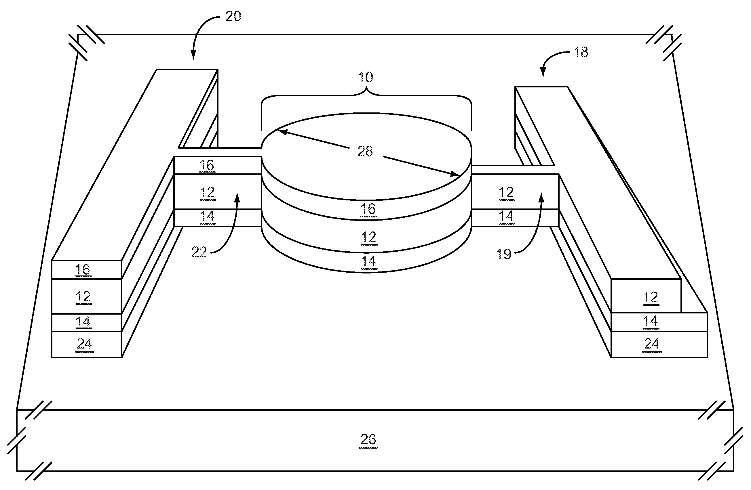
[0013]FIG. 1 shows a micro-electro-mechanical systems (MEMS) vibrating structure according to the present invention. The MEMS vibrating structure includes a single-crystal piezoelectric thin-film layer sandwiched between two conductive layers, such as metallization layers.

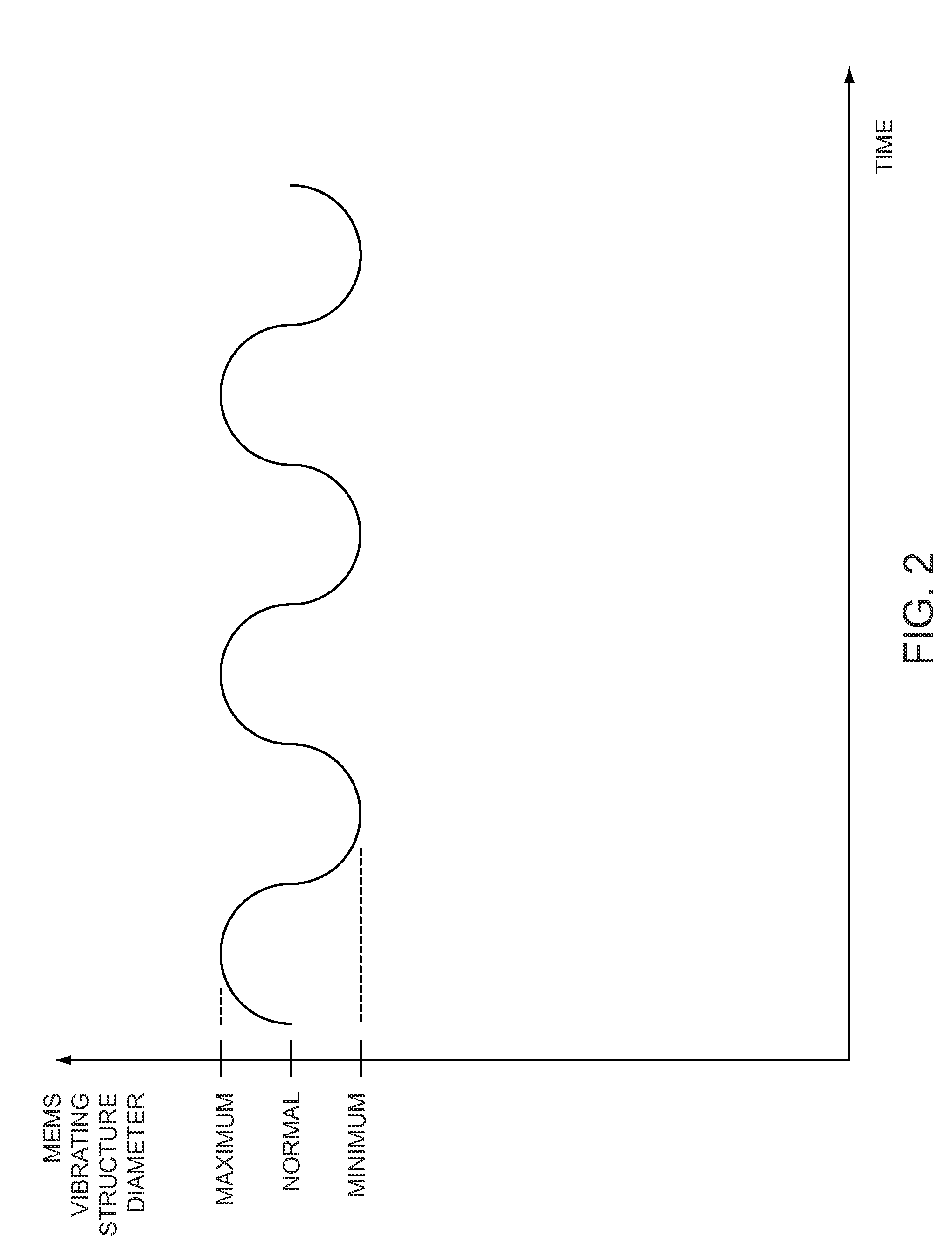
[0014]FIG. 2 is a graph illustrating how the MEMS vibrating structure diameter varies with time.

[0015]FIGS. 3A, 3B, 3C, 3D, 3E, and 3F show how a substrate and its layers are used to form the MEMS vibrating structure illustrated in FIG. 1, according to an exemplary embodiment of the present invention.

second embodiment

[0016]FIG. 4 shows a MEMS vibrating structure according to the present invention. The MEMS vibrating structure includes a single-crystal piezoelectric thin-film layer sandwiched between two conductive layers, such that one of the conductive layers is the principal resonating layer.

[0017]FIGS. 5A, 5B, 5C, 5D, 5E, and 5F show how a substrate and its layers are used to form the MEMS vibrating structure illustrated in FIG. 4, according to an exemplary embodiment of the present invention.

[0018]FIG. 6 shows a MEMS vibrating structure according to a third embodiment of the present invention. The MEMS vibrating structure includes a single-crystal piezoelectric thin-film layer sandwiched between two conductive layers, such that one of the conductive layers is attached to an additional layer, which is the principal resonating layer.

[0019]FIG. 7 shows a MEMS vibrating structure according to an alternate embodiment of the present invention.

[0020]FIG. 8 shows a top view of the MEMS vibrating str...


PUM


Abstract

The present invention relates to a micro-electro-mechanical systems (MEMS) vibrating structure having dominant lateral vibrations supported by a MEMS anchor system, and includes a single-crystal piezoelectric thin-film layer that has been grown with a specific crystal orientation. Since the MEMS vibrating structure has dominant lateral vibrations, its resonant frequency may be controlled by its size and shape, rather than layer thickness, which provides high accuracy and enables multiple resonators having different resonant frequencies on a single substrate.

Description

[0001]This application claims the benefit of provisional patent application Ser. No. 60 / 942,265, filed Jun. 6, 2007, the disclosure of which is hereby incorporated herein by reference in its entirety.FIELD OF THE INVENTION[0002]Embodiments of the present invention relate to micro-electromechanical systems (MEMS) vibrating structures, such as MEMS sensors, MEMS resonators, MEMS oscillators, or MEMS filters, which may be used in radio frequency (RF) communications systems.BACKGROUND OF THE INVENTION[0003]Resonators are devices that are often used in RF circuitry in frequency reference circuits and filter circuits. Generally, resonators need to be high-Q, low loss, stable, have a low temperature coefficient of frequency, have high repeatability, have high accuracy, and have a low motional impedance. Additionally, RF circuits often require multiple resonators having different resonant frequencies.[0004]One common type of resonator is a thin-film bulk acoustic resonator (FBAR), according...

Claims


Application Information

Patent Timeline
Patent Type & Authority Patents(United States)
IPC IPC(8): H01L41/08
CPCH03H3/0072H03H9/02275H03H9/02338H03H9/2436H03H2009/2442H03H2009/02496H03H2009/241
Inventor LI, SHENG-SHIANLEE, SEUNGBAEBHATTACHARJEE, KUSHAL
Owner QORVO US INC
Why Eureka
Try Eureka