Capping layer for a magnetic tunnel junction device to enhance dR/R and a method of making the same

a tunnel junction device and capping layer technology, applied in the field of high-performance magnetic tunnel junction elements and a method of making the same, to achieve the effect of low-magnetization capping

Active Publication Date: 2009-09-29
TAIWAN SEMICON MFG CO LTD
View PDF17 Cites 67 Cited by
  • Summary
  • Abstract
  • Description
  • Claims
  • Application Information

AI Technical Summary

Benefits of technology

[0013]One objective of the present invention is to provide a low magnetization capping layer in an MTJ element that is efficient in gettering oxygen atoms from an adjacent free layer.
[0014]A second objective of the present invention is to provide a low magnetization capping layer in accordance with the first objective that also blocks inter-diffusion between the capping layer and an adjacent free layer.
[0015]A third objective of the present invention is to provide a low magnetization capping layer in accordance with the second objective that enables the resulting MTJ element to achieve a high dR / R of about 30% or greater and an acceptable resistance (RA) value.

Problems solved by technology

The disadvantage of using a Ta capping layer is that Ta diffuses into NiFe during thermal annealing to produce an alloy that not only reduces free layer moment (Bs) but makes NiFe very magnetostrictive with a λS of ≧5×10⁻⁶.

Method used


Image

  • Capping layer for a magnetic tunnel junction device to enhance dR/R and a method of making the same
  • Capping layer for a magnetic tunnel junction device to enhance dR/R and a method of making the same
  • Capping layer for a magnetic tunnel junction device to enhance dR/R and a method of making the same

Examples


example 1

[0063]An experiment was conducted to determine the magnetic moment (Bs) of 500 Angstrom thick NiFeHf layers on a SiO2 / Si substrate that were co-sputtered using an Anelva C-7100-Ex Thin Film Sputtering System which consists of three 5PVD chambers each having five targets, an oxidation chamber, and a sputter etching chamber. At least one of the 5PVD chambers is capable of co-sputtering. The NiFe target and Hf target were arranged opposite each other at positions 2 and 4, respectively. The magnetic moment of each 500 Angstrom thick film shown in Table 1 was measured with a B—H looper.

[0064]

TABLE 1Bs (nanowebers) of 500 Angstrom Thick NiFeHf LayersNiFe power / Hf powerBs (as-deposited)Bs (annealed)NiFe (reference)10.810.8300 W / 300 Wnonenone300 W / 200 Wnone0.29400 W / 200 Wvery slight0.61600 W / 200 W0.540.89700 W / 200 W3.323.35800 W / 200 W3.473.64

[0065]Based on the Bs measurements, a nonmagnetic NiFeHf alloy, in the as-deposited state, is formed by co-sputtering NiFe(21%) and Hf targets with 300...

example 2

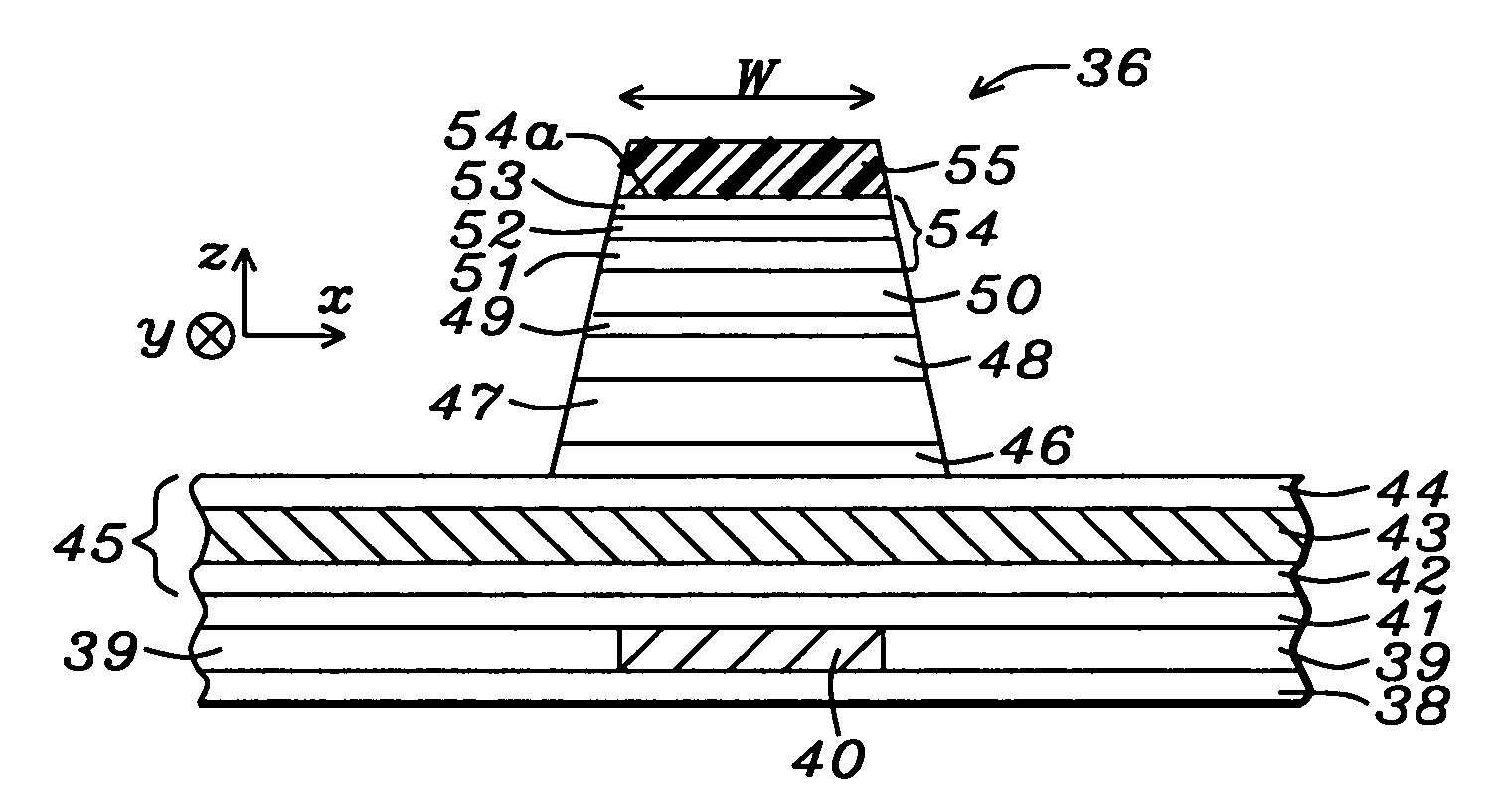
[0066]An unpatterned MTJ stack was formed on a substrate to determine the improvement in magnetic properties realized by incorporating a capping layer formed according to the present invention. In this example, the tunnel barrier layer is made of MgO and the free layer is a 33 Angstrom thick Ni79Fe21 layer. The capping layer has a NiFeHf / Ta / Ru configuration wherein the NiFeHf inner layer is about 25 Angstroms thick, the thickness of the Ta middle layer is 30 Angstroms, and the thickness of the Ru outer layer is 100 Angstroms. A standard capping layer represented by Ru30 / Ta30 / Ru100 was also deposited on the Ni79Fe21 free layer to serve as a reference as shown in rows 1 and 2 of Table 2. After all the films were deposited, the MTJ stack was annealed at 360° C. for 2 hours with an applied field of 10000 Oe. The results in Table 2 were obtained by using a B—H looper and a Capres CIPT (current in plane tunneling) to measure RA and dR / R. The other layers in the MTJ stack are the following...

example 3

[0070]An unpatterned MTJ stack was formed on a substrate to determine the improvement in magnetic properties realized by incorporating a capping layer formed according to the present invention. In this example, the tunnel barrier layer is made of AlOx and the free layer is a 33 Angstrom thick Ni79Fe21 layer. The tunnel barrier was formed by oxidizing an 8 Angstrom thick Al layer. The capping layer has a NiFeHf / Ta / Ru configuration wherein the NiFeHf inner layer is about 25 Angstroms thick, the thickness of the Ta middle layer is 30 Angstroms, and the thickness of the Ru outer layer is 100 Angstroms. A standard capping layer represented by Ru30 / Ta30 / Ru100 was also deposited on the Ni79Fe21 free layer to serve as a reference as shown in row 6 of Table 3. The seed layer, AFM layer, and pinned layer are the same as in Example 2. The MTJ stacks were annealed at 280° C. for 5 hours with an applied field of 10000 Oe.

[0071]

TABLE 3Magnetic properties of NiFe(free)-AlOxMTJs with different NiFe...


PUM


Abstract

An MTJ in an MRAM array or TMR read head is disclosed in which a low magnetization capping layer is a composite having a NiFeHf inner layer formed on a NiFe or CoFeB / NiFe free layer, a Ta middle layer, and a Ru outer layer on the Ta layer. For example, a low magnetization NiFeHf layer is achieved by co-sputtering NiFe and Hf targets with a forward power of 400 W and 200 W, respectively. A higher Hf content increases the oxygen gettering power of the NiFeHf layer and the thickness is modified to change dR / R, RA, and magnetostriction values. A so-called dead layer between the free layer and capping layer is restored by incorporating a NiFeHf layer on the free layer to improve lattice matching. The Fe content in the NiFe target used to make the NiFeHf layer is preferably the same as in the NiFe free layer.

Description

RELATED PATENT APPLICATIONS[0001]This application is related to the following: Ser. No. 10 / 868,715, filing date Jun. 15, 2004; and Ser. No. 10 / 844,171, filing date May 12, 2004.[0002]This application is also related to the following: Ser. No. 11 / 404,446, filing date Apr. 14, 2006, and Ser. No. 11 / 317,388, filing date Dec. 22, 2005 assigned to a common assignee.FIELD OF THE INVENTION[0003]The invention relates to a high performance Magnetic Tunneling Junction (MTJ) element and a method for making the same, and more particularly, to a capping layer comprised of a low magnetization NiFeHf layer formed adjacent to the free layer that serves as an oxygen getter agent and minimizes the “dead layer” between a free layer and capping layer.BACKGROUND OF THE INVENTION[0004]Magnetoresistive Random Access Memory (MRAM), based on the integration of silicon CMOS with MTJ technology, is a major emerging technology that is highly competitive with existing semiconductor memories such as SRAM, DRAM, ...

Claims


Application Information

Patent Timeline
Patent Type & Authority Patents(United States)
IPC IPC(8): H01L29/76H01L29/82
CPCB82Y25/00B82Y40/00G11B5/3906G11C11/16H01F10/30H01F41/302H01L43/10H01L43/12H01F10/3295H01F10/3259H01L27/222H01F10/3254G11C11/161G11C11/1673H10B61/00H10N50/01H10N50/85H10N50/10
Inventor HORNG, CHENG T.TONG, RU-YING
Owner TAIWAN SEMICON MFG CO LTD
Why Eureka
Try Eureka