Semiconductor device

a technology of serial interface and semiconductor, which is applied in the field of semiconductor devices having serial interfaces, can solve the problems of increasing the cost of the tester used for coping with the transfer frequency of high-speed serial data, and increasing the transfer frequency of serial data in high-speed serial interfaces. to achieve the effect of preventing the increase of test costs and reducing test costs

Active Publication Date: 2009-10-06
RENESAS ELECTRONICS CORP
View PDF13 Cites 10 Cited by
  • Summary
  • Abstract
  • Description
  • Claims
  • Application Information

AI Technical Summary

Benefits of technology

[0015]If a high-speed test with the transfer rate of, for example, the GHz order, is to be carried out, expensive high-speed testers are needed, thus leading to increased test costs and product costs.
[0024]According to the present invention, no costly high-speed tester is needed even in case of conducting a high-speed test of a serial interface to render it possible to reduce test cost or to prevent test costs from increasing.

Problems solved by technology

Recently, the transfer frequency for serial data in a high-speed serial interface has been increased to the extent that the test frequency of an LSI tester cannot cope with the transfer frequency for high-speed serial data.
Or, the cost of the tester used for coping with the transfer frequency for high-speed serial data would be prohibitive.
For this reason, it has not been possible to conduct tests for high-speed serial transmission or interrupts during field use.
If a high-speed test with the transfer rate of, for example, the GHz order, is to be carried out, expensive high-speed testers are needed, thus leading to increased test costs and product costs.
However, it is not possible to insert interrupt frames into through-frames to carry out testing.

Method used


Image

  • Semiconductor device
  • Semiconductor device
  • Semiconductor device

Examples


Embodiment Construction

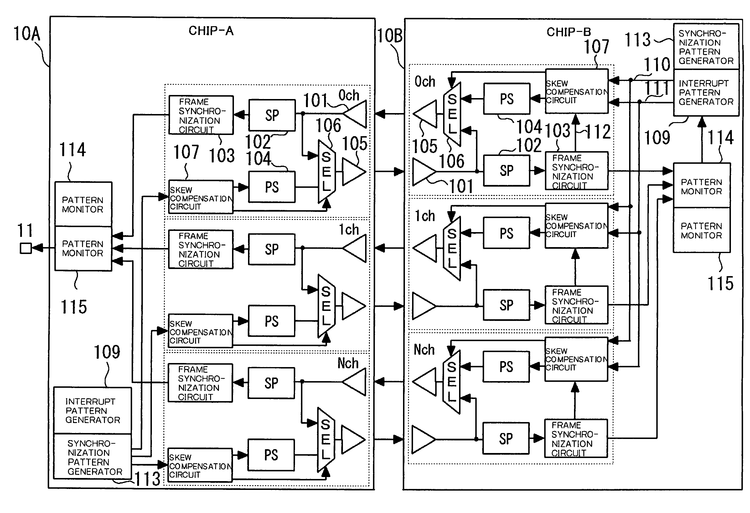
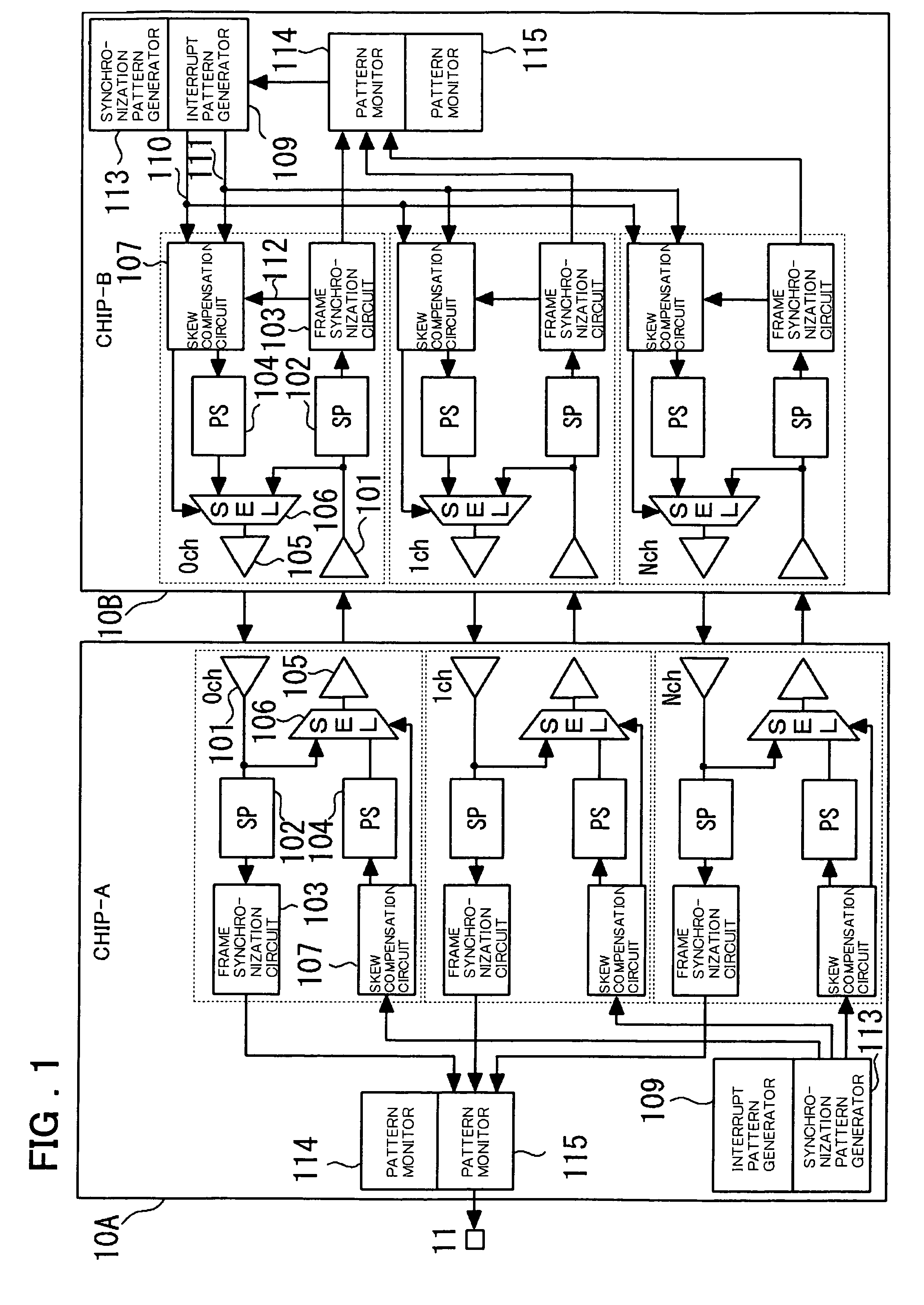
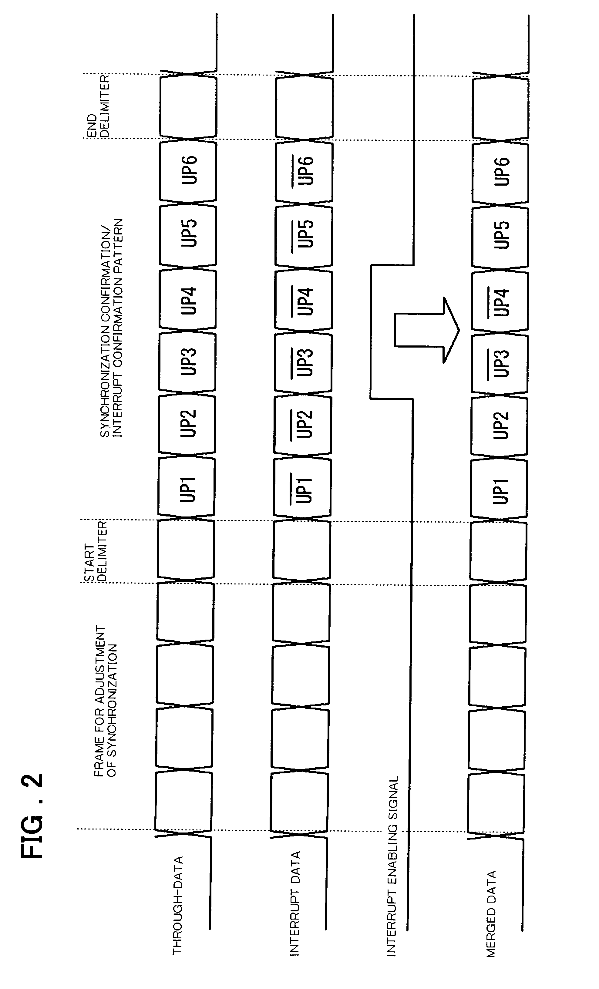
[0030]The present invention will now be described in further detail with reference to the accompanying drawings. Referring to FIG. 1, there are provided two semiconductor devices facing each other. Each of the semiconductor devices includes an interrupt pattern generator (109) for generating an interrupt enabling signal and interrupt data, and a selector (106) for receiving through-data from a path on which input serial data serially received is serially output unchanged, and serial data obtained on parallel-to-serial conversion of the interrupt data. The selector selects the through-data and the interrupt data when the interrupt enabling signal is in an inactive state and in an active state, respectively, and outputs the data selected. Each of the semiconductor devices also includes a circuit (114) for exercising control for instructing the interrupt pattern generator to generate the interrupt data and to activate the interrupt enabling signal in case the information instructing th...


PUM

PropertyMeasurementUnit
timeaaaaaaaaaa
speedaaaaaaaaaa
operation frequencyaaaaaaaaaa

Abstract

A semiconductor device including an interrupt pattern generator for generating an interrupt enabling signal and interrupt data, an input buffer for receiving input serial data, a selector, receiving through-data serially output from said input buffer and serial data obtained on parallel-to-serial conversion of said interrupt data, for selecting and serially outputting said through-data when said interrupt enabling signal is in an inactive state, and for selecting and serially outputting said interrupt data when said interrupt enabling signal is in an active state, and a circuit exercising control for instructing said interrupt pattern generator to generate said interrupt data and to activate said interrupt enabling signal in case the information instructing the merging of said interrupt data in a predetermined position of said through-data is detected from said input serial data.

Description

FIELD OF THE INVENTION[0001]This invention relates to a semiconductor device having a serial interface. More particularly, the present invention relates to a semiconductor device suited for testing.BACKGROUND OF THE INVENTION[0002]Recently, the operation frequency of semiconductor integrated circuits has been remarkably raised. For instance, in a serial interface, also termed ‘SerDes Interface’ or ‘Advanced Memory Buffer’, realizing high speed serial transfer in a gigabit range, such as DIMM (Dual Inline Memory Module), each channel includes a deserializer and a serializer. The deserializer recovers clock and data, synchronized with data which has been serially received by an input buffer to convert the recovered data into parallel data. The serializer converts the parallel data to be transmitted into serial data. In order to realize synchronized reception of the data among plural channels, frame synchronization patterns are periodically inserted at predetermined positions in the da...

Claims


Application Information

Patent Timeline
Patent Type & Authority Patents(United States)
IPC IPC(8): G11B20/20G11B20/02
CPCG01R31/31715
Inventor NISHIZAWA, MINORU
Owner RENESAS ELECTRONICS CORP
Why Eureka
Try Eureka