Wafer protective sheet

a protective sheet and wafer technology, applied in the field of wafer protective sheets, can solve the problems of easy scratching of stacked wafers, easy scratching of recessed parts of protective sheets, and negative impact of wafer fibers, so as to reduce the possibility of making scratches on the wafer, prevent effective adhesion, and facilitate automatic handling

Active Publication Date: 2009-11-03
ACHILLES CORP
View PDF6 Cites 12 Cited by
  • Summary
  • Abstract
  • Description
  • Claims
  • Application Information

AI Technical Summary

Benefits of technology

[0009]In order to accomplish the above object, the inventors of the present invention have conducted research for characteristics required of wafer protective sheets. As a result, the inventors found that a type of wafer protective sheet can prevent wafers from being scratched and that it does not adhere to wafers and is accordingly easy to be handled by an automatic machine. This type of wafer protective sheet has a large number of alternately arrayed projected parts and recessed parts, and has such an appropriate bending resistance as the wafer protective sheet turns flat or substantially flat with the projected parts and recessed parts pressed while a pressure is being applied to stacked wafers in a container in their thickness direction, and as the projected parts and recessed parts are restored to the original state when the container is uncovered to remove the pressure. The inventors also found that the wafer protective sheet can be made of a synthetic resin sheet having a bending resistance and satisfying characteristics required of the wafer protective sheet even if its thickness is reduced to 130 μm or less, preferably 110 μm or less. Thus, the present invention was accomplished.
[0011]Since the wafer protective sheet of the present invention is made of a synthetic resin with a thickness of 80 to 130 μm whose bending resistance has been set at 30 to 80 mm by providing the projected parts and recessed parts, the wafer protective sheet has such a flexibility as projected parts and recessed parts turns flat or substantially flat when a pressure of, for example, 1×10³ to 1×10⁴ Pa, is applied to wafers in a container in the thickness direction of the wafers so that the wafers do not move. Thus, the possibility of making scratches on the wafers is reduced, and adhesion can be prevented effectively because the projected parts and recessed parts are restored to the original state when the container is opened.
[0012]In addition, in the wafer protective sheet of the present invention, the large number of projected parts and recessed parts are alternately arrayed in such a manner as to be positioned at intersections of lattice stripes. Consequently, the bending resistances in the lengthwise and crosswise directions of the wafer protective sheet are substantially the same; hence stiffness of the sheet has no orientation. Furthermore, since the projected parts are formed on both the front surface and the rear surface so that the resulting sheet has no distinction between the front surface and the rear surface, the wafer protective sheet can be more easily handled automatically.

Problems solved by technology

Unfortunately, the stacked wafers are liable to get scratched by their rubbing against each other.
In this instance, if the wafer protective sheets are hard, the projected parts and recessed parts of the protective sheets easily make scratches on the wafers.
However, fibers from such wafer protective sheets may negatively affect the wafers due to drop-out of fibers from the wafer protective sheet.
However, this results in high cost, disadvantageously.

Method used


Image

  • Wafer protective sheet
  • Wafer protective sheet
  • Wafer protective sheet

Examples


example

[0034]Into 100 parts by weight of each synthetic resin (high density polyethylene) shown in Table 1 was added 15 parts by weight of a polymeric antistatic agent (PELESTAT 300 produced by Sanyo Chemical Industries, Ltd.) and 1 part by weight of a black pigment. Synthetic resin compounds having flexural modulus shown in Table 1 were thus prepared. The synthetic resin compounds were each formed into a synthetic resin sheet with a thickness t shown in Table 1 by extrusion method.

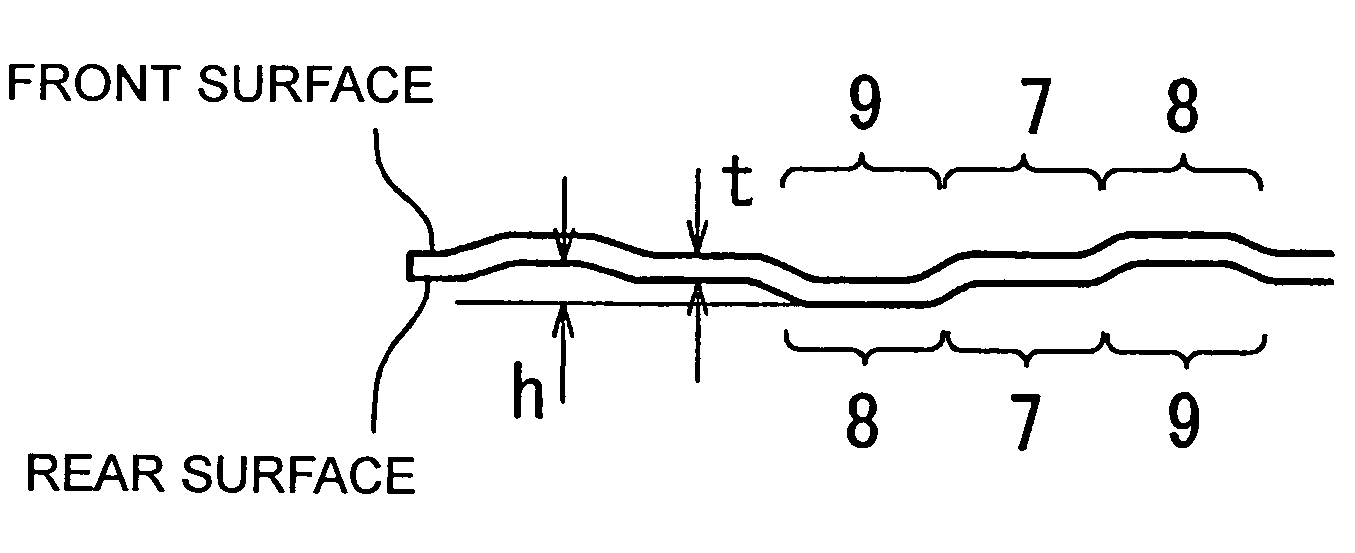
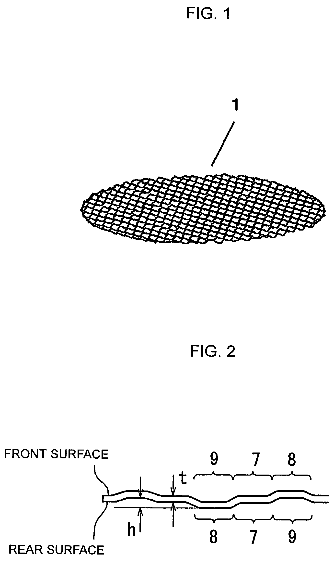
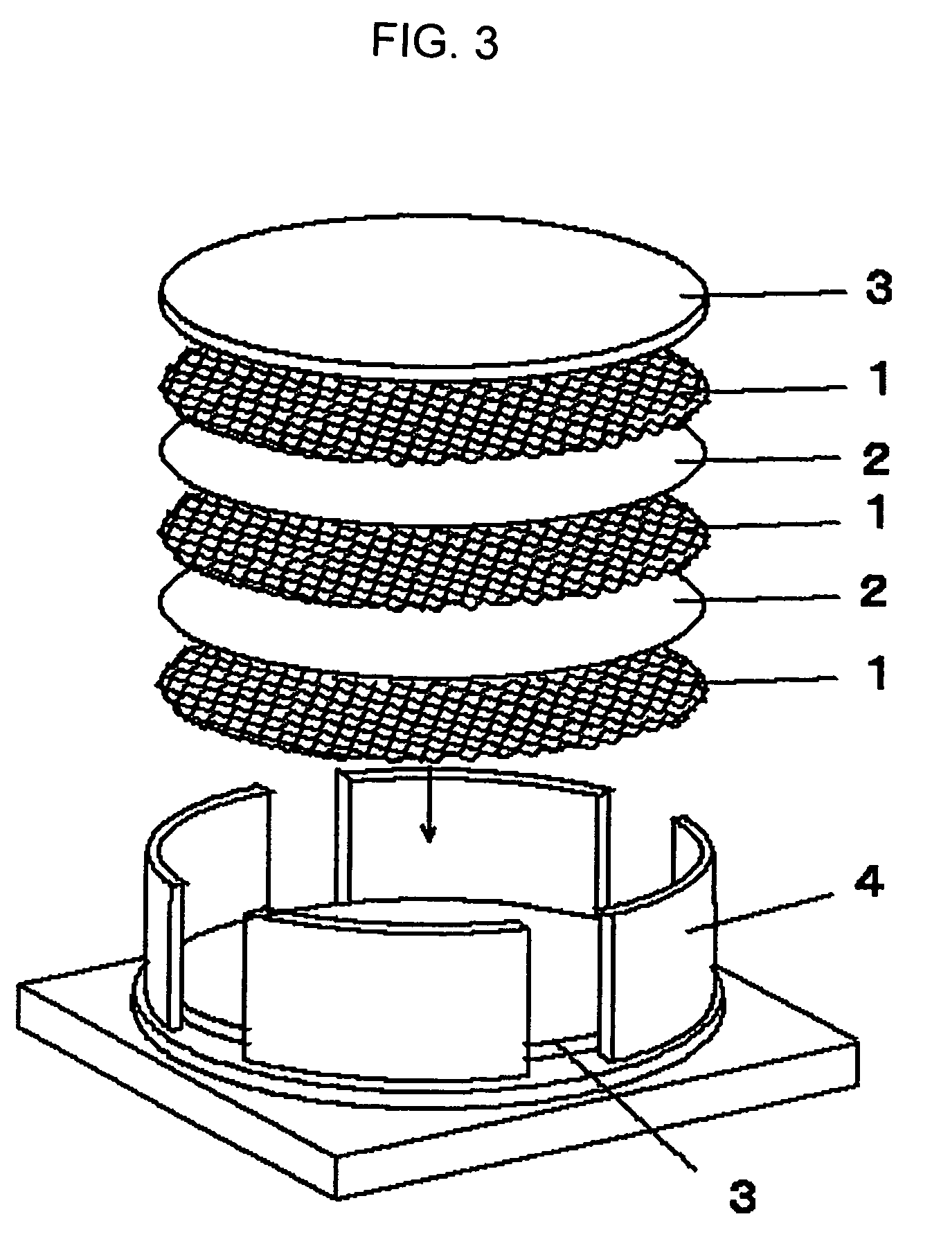
[0035]The synthetic resin sheet was heated and subjected to embossing with a pair of rolls having many protrusions. The projected parts and the recessed parts were alternately formed in lattice stripes manner on the sheet. The resulting sheet was cut into wafer protective sheets 1 with a press cutting machine of 8 inches in diameter. The height h of the projected parts and recessed parts was 25 μm; the area of each projection or recess was 1.5 mm2 in plan view; the density of the projected parts and recessed par...


PUM

PropertyMeasurementUnit
thicknessaaaaaaaaaa
flexural modulusaaaaaaaaaa
heightaaaaaaaaaa

Abstract

A wafer protective sheet 1 is made of a synthetic resin sheet with a thickness of 80 to 130 μm having a large number of projected parts and recessed parts on its front and rear surfaces. The large number of projected parts and the large number of recessed parts are respectively disposed so that each part is positioned at intersections of lattice stripes, and the projected part and the recessed part are disposed alternately each other. The sheet has such a water-like cross section that the recessed parts in the rear surface match the projected parts on the front surface and the projected parts on the rear surface match the recessed parts in the front surface. The wafer protective sheet 1 has a bending resistance of 30 to 80 mm. The wafer protective sheet 1 of the present invention is sufficiently thin. When the wafer protective sheets are interposed between stacked wafers to protect them, the sheets do not adhere to the wafers. Thus, wafers housed in a container can be protected against vibration during transportation.

Description

TECHNICAL FIELD[0001]The present invention relates to a wafer protective sheet for protecting semiconductor wafers that are stacked on top of one another in a container.BACKGROUND ART[0002]A semiconductor wafer (hereinafter referred to as a wafer) is generally a thin disk cut out of a silicon single-crystal ingot, having a diameter of, for example, about 2 to 12 inches. The wafer is provided with many circuits, such as those for LSI's, on its surface and is then cut into chips. The chips are packaged, thus producing semiconductor devices, such as LSI's.[0003]In the above process, the steps of cutting wafers out of the ingot, providing circuits on the wafers, and cutting the wafers into chips and packaging them are often performed in different places. For the transportation of the wafers from a place where one of the above-mentioned steps is carried out to another place, a special container of the wafers which is manufactured for such transportation is generally used.[0004]For exampl...

Claims


Application Information

Patent Timeline
Patent Type & Authority Patents(United States)
IPC IPC(8): B32B1/00B65D85/00H01L21/00H01L21/673
CPCH01L21/67132H01L21/67369Y10T428/24669Y10T428/24628Y10T428/216
Inventor FUYUMURO, MASAHIKONAKAYAMA, YOSHITAKAKAWASHIMA, EIICHI
Owner ACHILLES CORP
Why Eureka
Try Eureka