Dual damascene patterning method

a patterning and damascene technology, applied in the direction of electrical equipment, semiconductor devices, semiconductor/solid-state device details, etc., can solve the problems of new problems in semiconductor processing, low-k damage, photoresist poisoning, etc., to eliminate photoresist poisoning, avoid (or at least minimize) low-k damage, and eliminate resist poisoning

Inactive Publication Date: 2009-11-03
INTERUNIVERSITAIR MICRO ELECTRONICS CENT (IMEC VZW)
View PDF13 Cites 4 Cited by
  • Summary
  • Abstract
  • Description
  • Claims
  • Application Information

AI Technical Summary

Benefits of technology

[0021]More particularly, a metal hardmask based patterning method is provided which allows elimination of resist poisoning while avoiding (or at least minimizing) low-k damage.
[0022]A method according to a preferred embodiment can be used to eliminate photoresist poisoning in dual damascene patterning, in particular to eliminate or reduce the photoresist poisoning for trench etching over a via as performed in a via-first approach, while avoiding or at least minimizing plasma damage to the sidewalls, in particular the sidewalls of the trenches in the via-first approach used for dual damascene patterning.
[0036]The anisotropical etching chemistry used for etching said second hole in said dielectric layer present the advantage of avoiding or at least minimizing plasma damage to the sidewalls of the hole in the dielectric material.

Problems solved by technology

The use of these (porous) low-k materials as dielectric materials in interconnect structures brings new issues to the semiconductor processing.
Examples of these issues include photoresist poisoning and low-k damage due to etch, ash and / or clean processes.
Photoresist poisoning is a particular problem when 248 nm (DUV) or 193 nm (ArF) wavelength photoresists are used in conjunction with porous low-k materials.
The altered photoresist material may not be lithographically patterned as expected and result in imprecisely formed features in the photoresist material or excessive photoresist residue remaining on the substrate surface after photoresist development, both of which can detrimentally affect subsequent processes, such as etching processes.
With the via-first approach for dual damascene patterning, the use of photoresist layers on dielectric layers often results in “poisoning” of the line imaging resist which is done after vias are fully or partially etched into the dielectric.
The poisoning problem appears to be much worse when the dielectric layer is a porous low-k insulator applied using chemical vapor deposition (CVD), as compared to silicate glass dielectric layers.
Another important issue in integrating low-k dielectrics is the plasma damage caused by etching, stripping and post etch cleaning.
The use of oxygen containing etch / strip chemistries typically results in depletion of the carbon present in the film, making the film hydrophilic and susceptible to water (k value>>80) adsorption, which leads to an increase of the k-value of the film.
This problem is becoming even more important with the miniaturization of ICs where the feature size becomes comparable to the damaged region.
Several approaches are described in the state of the art to solve the poisoning problems but these are incomplete and too complicated.
However, such resist materials compromise imaging resolution and decrease lithographic process window.
However, such modifications may adversely affect the dielectric constant and other characteristics of the insulating materials.
Since it is difficult to deposit materials in high-aspect ratio vias, this approach may not be extendable to future technologies.
Defects in thin regions of this liner may allow poisoning gases to pass through, and even with low statistical occurrence may cause an unacceptable level of defective patterns in the line imaging layer.
This is however not without the risk of damaging the low-k material and increasing the k-value of the bulk low-k material.
This approach is only valid for single damascene processing and not applicable for etching a trench over a patterned via structure with the via-first approach in dual damascene processing.
In the case of CVD low-k materials, this oxidizing plasma will cause low-k damage to the sidewalls of the trenches.
After trench etching there is still a considerable amount of barrier layer and resin layer that needs to be removed by means of a wet stripping process (oxidizing solution containing H2SO4 / H2O2) which involves a further risk of low-k damage.
Thus, the prior art proposes several solutions for eliminating resist poisoning but all of them do have serious drawbacks and shortcomings.
The prior art does never provide a solution that simultaneously solves the problem of eliminating photoresist poisoning and avoiding or at least minimizing plasma damage of the dielectric material.
On the contrary, some of the prior art solutions to avoid photoresist poisoning create low-k damage.

Method used


Image

  • Dual damascene patterning method
  • Dual damascene patterning method
  • Dual damascene patterning method

Examples


example

Example 1

Processing a Dual Damascene Structure on a Substrate Avoiding Resist Poisoning and Reducing Plasma Damage to the Side Walls of the Trench

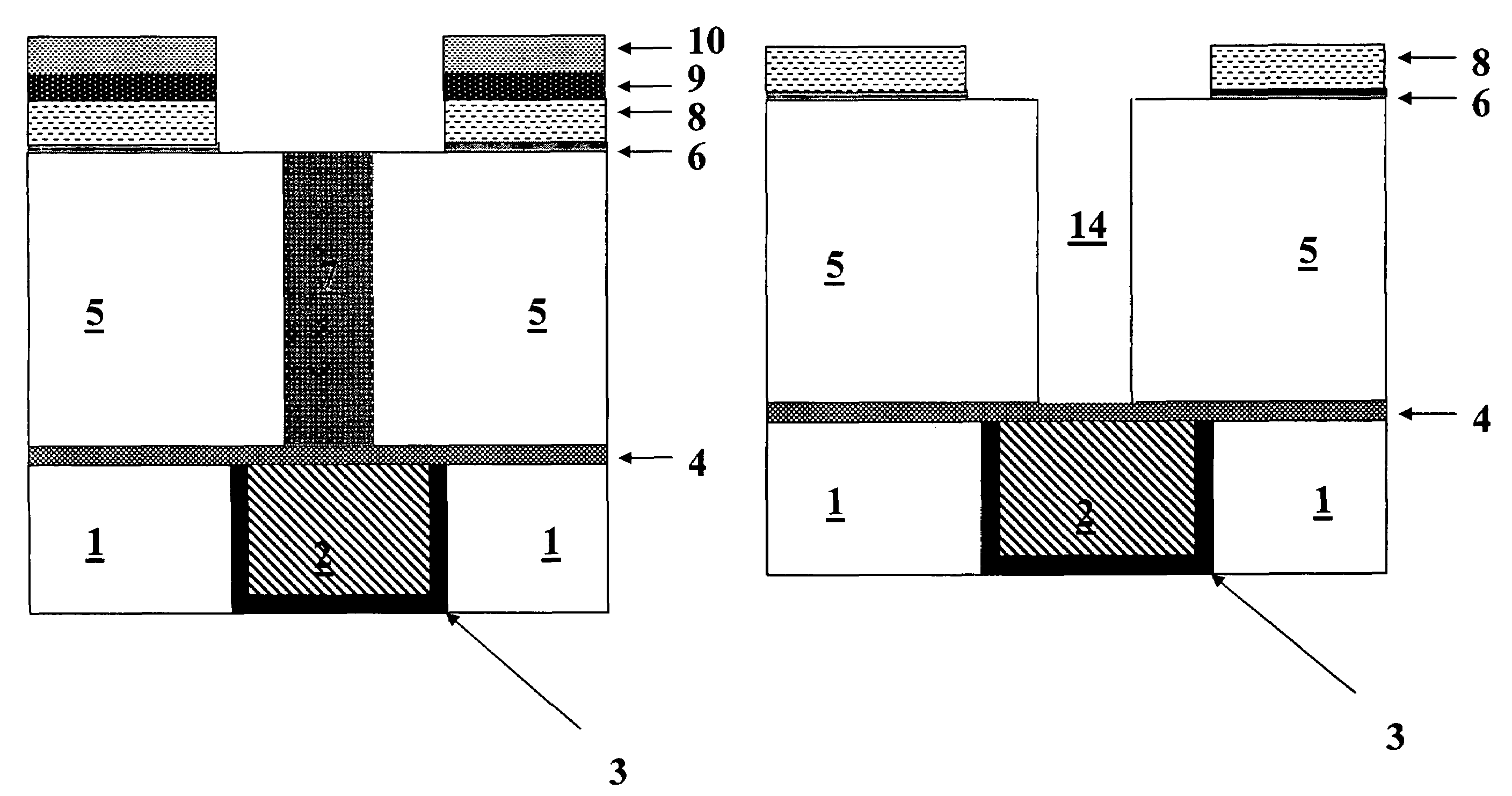
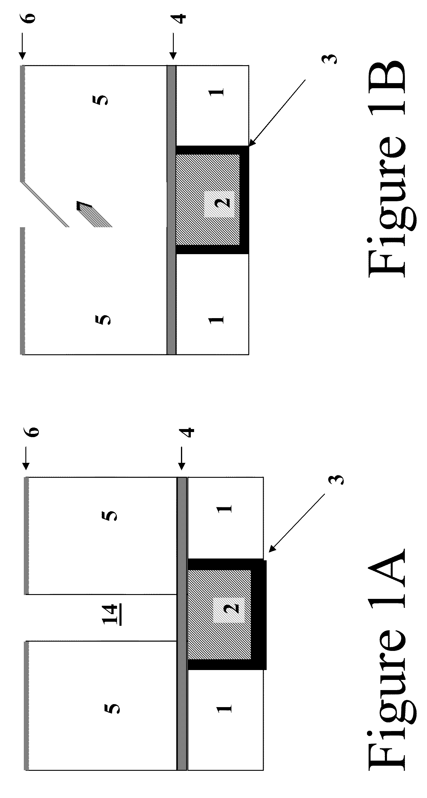
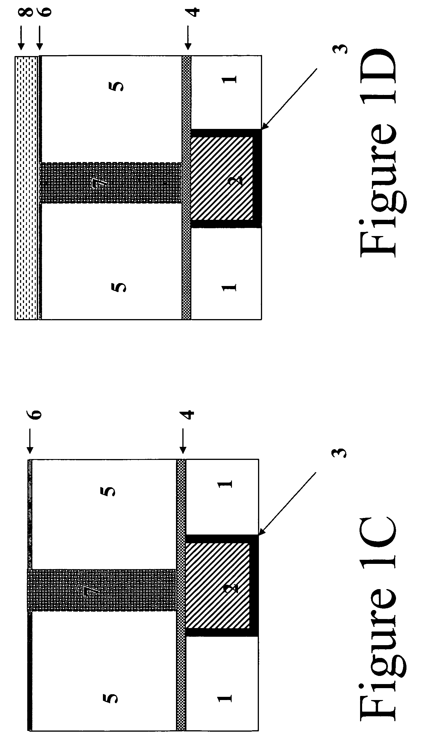
[0186]The method, based on the process flow described, is illustrated in this example.

[0187]The patterning of the trench (second hole) was done with a hardmask selective etch plasma comprising C4F8 without oxygen to avoid possible side wall damage of the trench during patterning.

[0188]The resist was stripped before the patterning of the trenches.

[0189]The dual damascene stack consisted of 30 nm SiC, 340 nm SiOC (k-value˜3.0) and a 13 nm oxide cap. The via photo, with 100 nm target dimension, was exposed using a 20 nm thick BARC layer and 220 nm resist. Minimum via pitch was 200 nm.

[0190]The via holes, including the SiC bottom layer opening, were etched as follows: 10 sec. BARC opening in CF4 / O2; 15 sec. via etching (step 1) in Ar / O2 / C4F8; 20 sec. via etching (step 2) in Ar / N2 / C4F8 / CH2F2; and 10 sec. resist strip in O2 / CF4

[0191]The vias we...


PUM


Abstract

A method for patterning a dual damascene structure in a semiconductor substrate is disclosed. The patterning is a metal hardmask based pattering eliminating at least resist poisoning and further avoiding or at least minimizing low-k damage. The method can be used as a full-via-first patterning method or a partial-via-first patterning method.

Description

RELATED APPLICATION[0001]This application claims the benefit of U.S. Provisional Application No. 60 / 669,973, filed Apr. 11, 2005. The above-referenced prior application is incorporated by reference herein in its entirety and is hereby made a portion of this specification.FIELD OF INVENTION[0002]The present invention is related to the field of patterning dual damascene interconnect structures. The present invention is further characterized in eliminating photoresist poisoning and avoiding, or at least minimizing, low-k damage during patterning.BACKGROUND OF THE INVENTION[0003]The semiconductor industry is continuously reducing the dimensions of the devices. In Back End Of Line (BEOL) processing it concerns the reducing dimensions of conductive layers as well as the separation of the different conductive structures to each other. Lowering the capacitance in between these structures becomes extremely important and low-k materials replace conventional dielectric insulating materials. Th...

Claims


Application Information

Patent Timeline
Patent Type & Authority Patents(United States)
IPC IPC(8): H01L21/4763
CPCH01L21/76808H01L21/7681H01L23/53295H01L23/53238H01L21/76813H01L2924/0002H01L2924/00
Inventor OLMEN, JAN VANHOVE, MARLEEN VANSTRUYF, HERBERTHENDRICKX, DIRKVANHAELEMEERSCH, SERGEBOULLART, WERNER
Owner INTERUNIVERSITAIR MICRO ELECTRONICS CENT (IMEC VZW)
Why Eureka
Try Eureka