Memory device, current sense amplifier, and method of operating the same

a current sense amplifier and memory device technology, applied in the field of current sense amplifier circuits, can solve the problems of large capacitance load of memory cells, excessive amount of time needed to read memory cells, and inability to provide enough cell current, etc., to achieve the effect of increasing circuit stability and speed, improving mismatch tolerance, and reducing the threshold voltage associated

Inactive Publication Date: 2009-11-10
MONTEREY RES LLC
View PDF25 Cites 18 Cited by
  • Summary
  • Abstract
  • Description
  • Claims
  • Application Information

AI Technical Summary

Benefits of technology

[0017]According to one embodiment, a current sense amplifier (ISA) circuit is provided herein for improving mismatch tolerance and increasing circuit stability and speed. In general, the current sense amplifier circuit may include a pair of cross-coupled transistors, a pair of output nodes and a first pair of load transistors. The pair of cross-coupled transistors may be coupled for receiving a pair of differential currents and for generating a pair of differential voltages, which may then be supplied to pair of output nodes. The first pair of load transistors may have mutually-connected gate terminals, mutually-connected drain terminals, and a source terminal coupled to a different one of the output nodes. In some cases, an enable transistor may be coupled between the mutually-connected drain terminals of the first pair of transistors and ground. The enable transistor may be configured for activating the current sense amplifier circuit upon receiving a sense enable signal at a gate terminal thereof.
[0018]In some cases, the source and body terminals of the first pair of load transistors may be coupled together to reduce a threshold voltage associated with the transistors. This allows the current sense amplifier to operate under low power supply conditions (e.g., down to about 0.7V, in some embodiments).
[0019]In some cases, a second pair of load transistors may be added to the current sense amplifier circuit. For example, each of the second pair of load transistors may be coupled in parallel to a different one of the first pair of load transistors, and in series between a different one of the output nodes and the enable transistor. In some cases, a digital control signal may be supplied to the gate terminals of the second pair of load transistors to increase circuit stability and / or speed. For example, the second pair of load transistors may be deactivated upon receiving a first logic value of the digital control signal to increase circuit stability at low power supply values (e.g., about 1.2V and below, in some embodiments). On the other hand, a second logic value of the digital control signal may be used to activate the second pair of load transistors to increase circuit speed at high power supply values (e.g., above 1.2V, in some embodiments).
[0020]In some cases, an equalization transistor may be added between the output nodes of the current sense amplifier circuit. When activated, the equalization transistor may be used for equalizing the pair of differential voltages for a predetermined amount of time at the beginning of a sense cycle. For example, a delay circuit may be added to the current sense amplifier for supplying a delayed version of the sense enable signal to a gate terminal of the equalization transistor. The delayed version of the sense enable signal may be used for deactivating the equalization transistor after the predetermined amount of time, so that the pair of differential voltages may be accurately represented at the pair of output nodes.
[0021]In general, the predetermined amount of time may begin once the current sense amplifier is activated and may end once the equalization transistor is deactivated. In some cases, the predetermined amount of time may be based on an amount of fabrication-related mismatch between corresponding transistors within differential portions of the current sense amplifier circuit. Equalizing the differential voltages during this time period allows current to fully develop within the ISA before the true voltage differential is output for amplification. In other words, equalization may be used to prevent the “double switching” that often occurs at the beginning of a sense cycle (due to transistor mismatch) by preventing the ISA from generating erroneous results during the predetermined time period.

Problems solved by technology

However, the bitline may be quite long in some memory devices (e.g., large memory arrays), resulting in a large capacitive load for the memory cell.
In some cases, the memory cell may not be able to provide enough cell current to quickly discharge or charge a large bitline, and an excessive amount of time may be needed to read the memory cells.
Therefore, voltage sensing may not be the preferred sensing scheme in some memory devices (e.g., when operation speed is of concern).
However, transistors M1 and M2 are not the only devices to suffer from mismatch—transistors M3 / M4 and devices in the memory cell may suffer, as well.
In some cases, transistor mismatch may cause the sense amplifier to detect the wrong voltage at the beginning of a sense cycle.
For example, the differential currents initially supplied to the current sense amplifier may be relatively weak.
During this time (i.e., at the start of a sense cycle), transistor mismatch may cause more current to flow in one leg of the sense amp than the other, thereby causing the sense amplifier output to “go in the wrong direction” until the differential currents are firmly established.
Another disadvantage of the conventional circuit of FIG. 2 is that the optimal size of the PMOS load transistors (M3 and M4) is a strong function of VCC for speed and stability.
As such, it is often difficult to achieve high performance across a wide range of power supply voltages (VCC) with the same load.
In addition to speed and stability concerns, the circuit performance tends to suffer (or even fail) at lower power supply voltages (e.g., about 1.2V and lower).

Method used


Image

  • Memory device, current sense amplifier, and method of operating the same
  • Memory device, current sense amplifier, and method of operating the same
  • Memory device, current sense amplifier, and method of operating the same

Examples


Embodiment Construction

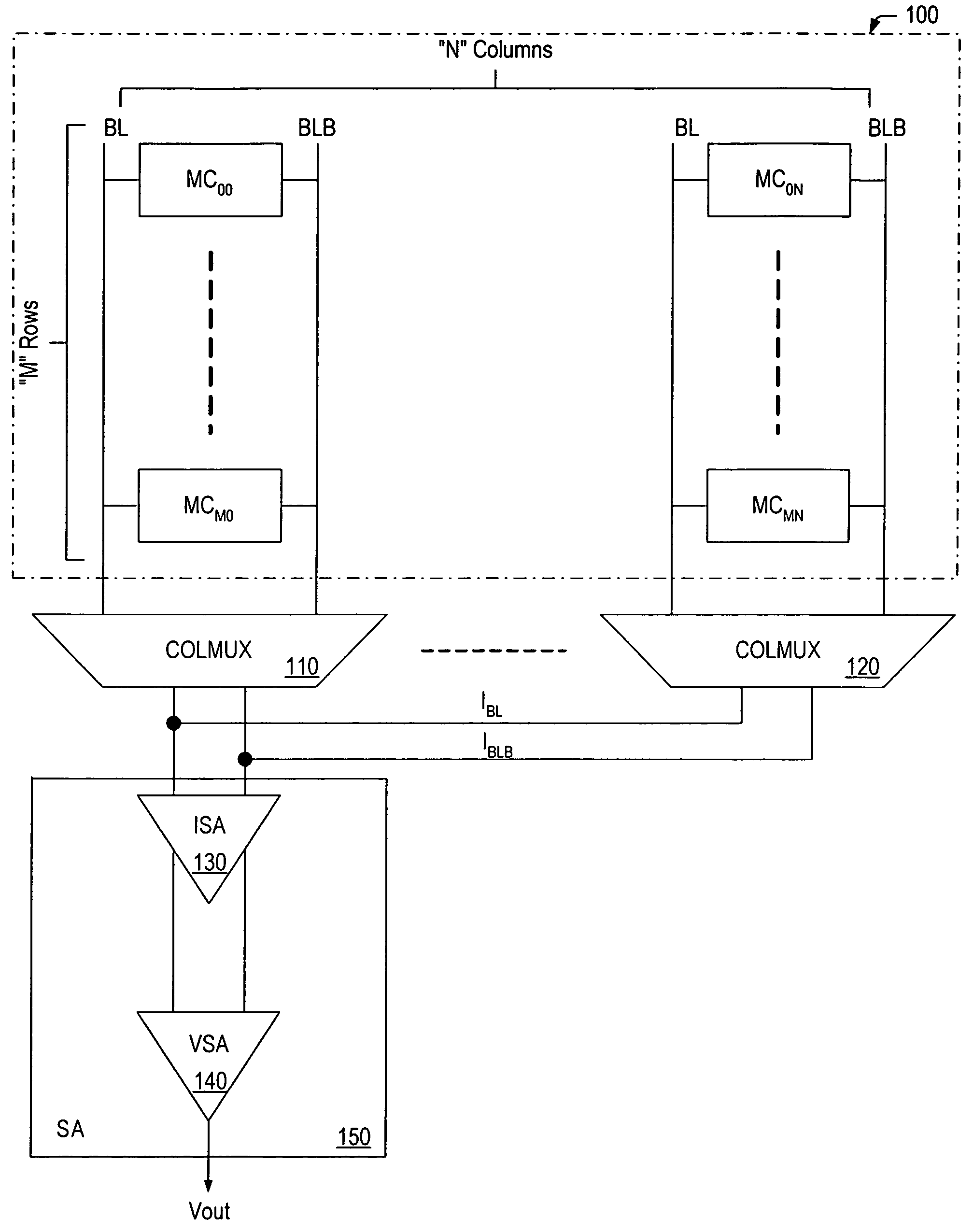
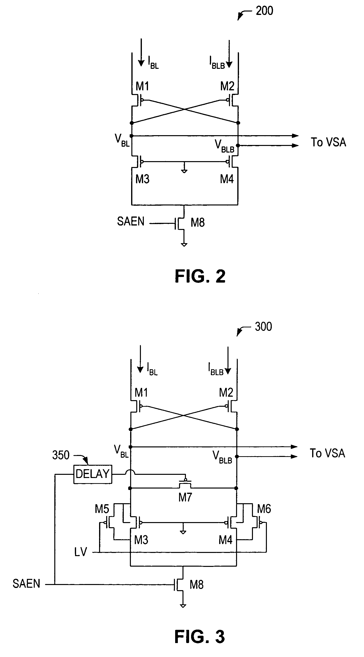
[0033]One embodiment of an improved current sense amplifier 300 is described and shown in FIG. 3. The improved current sense amplifier is well suited for use in a memory device, and in one preferred application, may be used within a high speed dual-port static RAM (SRAM) device. However, it is noted that the inventive concepts described herein are not limited to a particular memory device, and instead, may be applied to various types of memory (including, but not limited to, types of ROM, RAM, and FLASH memories), as well as other applications (such as programmable arrays).

[0034]As noted above, even symmetrical sense amp designs may suffer the effects of transistor mismatch during the initial stages of a sense cycle. Transistor mismatch becomes more of a problem as transistor sizes decrease and / or the size of memory arrays increase. For example, a typical memory device may exhibit up to + / −3 sigma (standard deviations) of transistor mismatch due, in part, to the high volume of memor...


PUM


Abstract

A memory device, current sense amplifier and method of operating the same are disclosed herein. In accordance with one embodiment, the current sense amplifier circuit may include a pair of cross-coupled transistors, a pair of output nodes and a first pair of load transistors. The pair of cross-coupled transistors may be coupled for receiving a pair of differential currents and for generating a pair of differential voltages, which may then be supplied to the pair of output nodes. The first pair of load transistors may have mutually-connected gate terminals, mutually-connected drain terminals, and a source terminal coupled to a different one of the output nodes. In a unique aspect of the invention, an equalization transistor may coupled between the pair of output nodes for equalizing the pair of differential voltages for a predetermined amount of time at the beginning of a sense cycle. As such, the equalization transistor may be added to prevent the current sense amplifier circuit from generating erroneous results during the predetermined time period.

Description

PRIORITY APPLICATION[0001]The present application claims priority to Ser. No. 60 / 623,525 filed Oct. 29, 2004 entitled “Current Sense Amplifier (ISA) Circuit that is Mismatch Tolerant Over a Wide VCC Range” by Peng et al.BACKGROUND OF THE INVENTION[0002]1. Field of the Invention[0003]This invention relates to electronic circuits and, more particularly, to current sense amplifier circuits used in semiconductor devices.[0004]2. Description of the Related Art[0005]The following descriptions and examples are given as background only.[0006]Many modern semiconductor memories employ differential bit lines and some sort of differential amplifier or sensing circuit in their design. These differential amplifiers and sense circuits are commonly known as sense amplifiers (or “sense amps”). In addition to memory devices, sense amplifiers may be used in programmable arrays and many other applications. A wide variety of sense amps are known in the art, including current sensing and voltage sensing ...

Claims


Application Information

Patent Timeline
Patent Type & Authority Patents(United States)
IPC IPC(8): G11C7/02
CPCG11C7/062G11C7/08G11C2207/063
Inventor PENG, TAOLANDRY, GREG J.
Owner MONTEREY RES LLC
Why Eureka
Try Eureka