Semiconductor element, electronic device

a technology of electromagnetic elements and semiconductors, applied in the direction of identification means, instruments, television systems, etc., to achieve the effects of simple structure, constant intensity, and decreased luminous intensity

Inactive Publication Date: 2009-12-08
SEMICON ENERGY LAB CO LTD
View PDF46 Cites 11 Cited by
  • Summary
  • Abstract
  • Description
  • Claims
  • Application Information

AI Technical Summary

Benefits of technology

[0025]In view of the above, an object of the invention is to provide a light-emitting device with a simple structure in which a luminous element can maintain an almost constant intensity without depending on ambient temperature and without greatly decreasing the luminous intensity as the time elapses. Another object of the invention is to provide alight-emitting device with a simple structure in which desired color display is possible without any color shift. Yet another object of the invention is to provide a structure of a semiconductor element available to put the above-mentioned light-emitting device into practice and an electric circuit using the semiconductor element.
[0032]The invention further provides an electric circuit using a writing element and a driving element. A multi-drain transistor is used in one or both of the writing and driving elements. The invention having such structure contributes to simplification, reduction in the area and high integration of a circuit requiring a current storing function.
[0033]The invention also provides a display device having a pixel provided with a current-driving type of displaying element, the above pixel comprising a writing element for selecting input of a video signal in a form of a current value for the pixel and a driving element for controlling the amount of electric current flowing to the displaying element, wherein a semiconductor element is used in at least one of the writing element and the driving element. The invention is especially effective when the displaying element has a characteristic that its resistant value changes in accordance with the change in temperature or time. That is, the value of the current flowing to the displaying element can be kept constant without depending on the change in temperature or time, so that the intensity can be kept good. It is most effective that the displaying element is a luminous element since the luminous element has a characteristic of depending on the change in temperature or time.

Problems solved by technology

The elements other than the luminous element are generally formed by means of a TFT, which is, however, disadvantageous since the number of TFT increases and the circuit area including wiring thereby increases.

Method used


Image

  • Semiconductor element, electronic device
  • Semiconductor element, electronic device
  • Semiconductor element, electronic device

Examples


embodiment mode 1

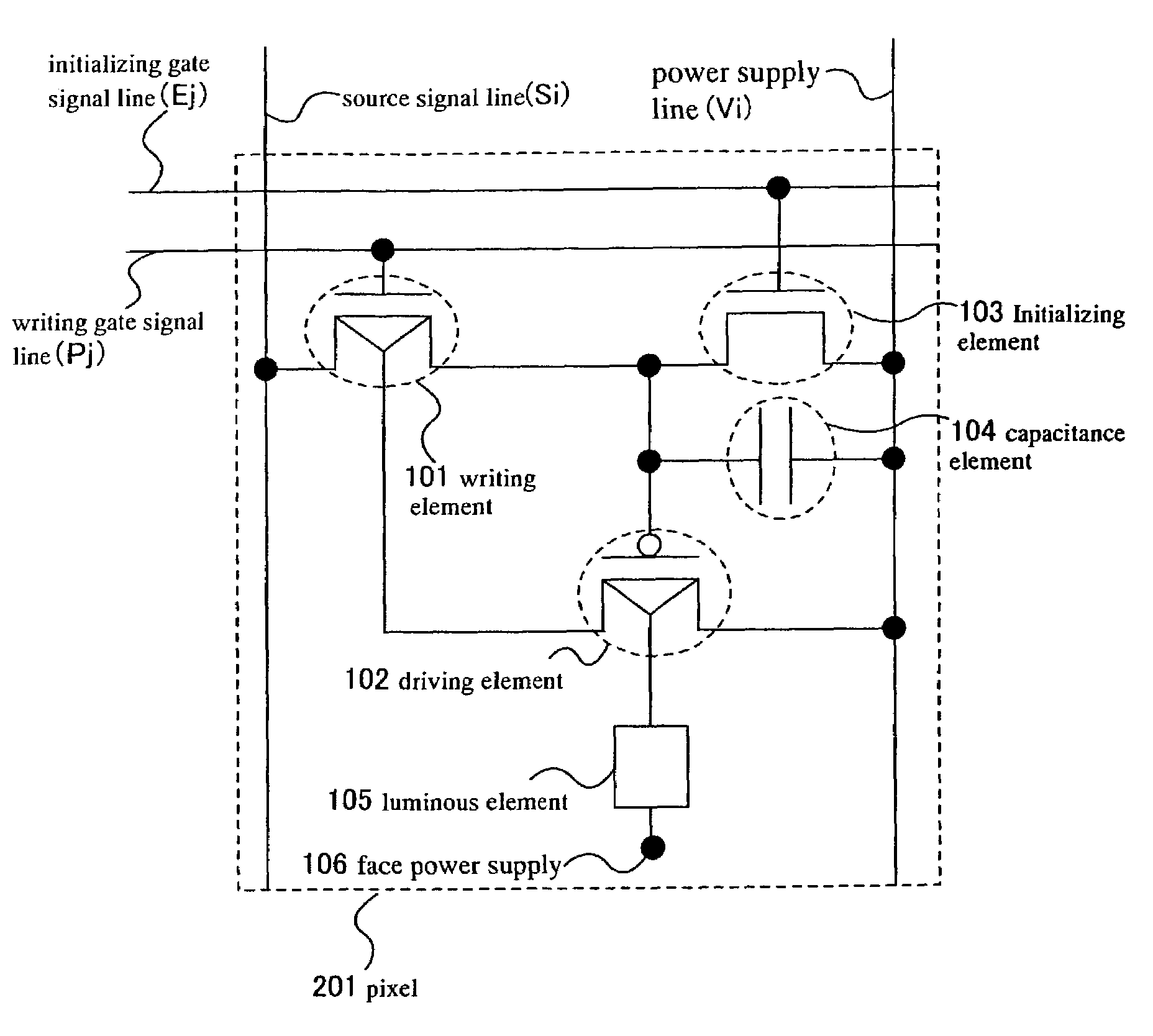
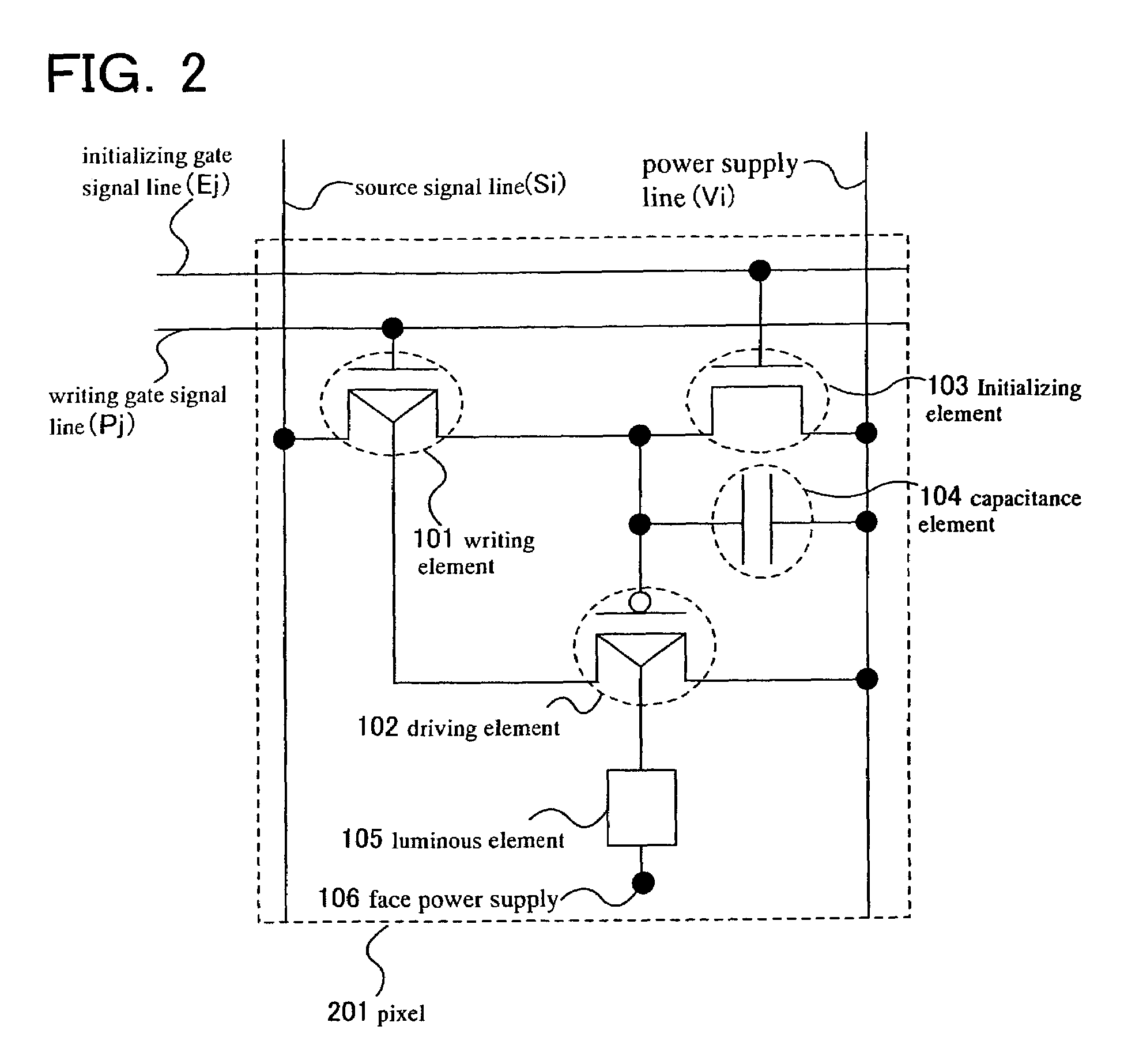
[0054]FIG. 2 shows an example of a pixel circuit with a current storing function in a light-emitting device according to the invention.

[0055]A pixel 201 shown in FIG. 2 has a source signal line Si (one of S1 to Sx), a writing gate signal line Pj (one of P1 to Py), an initializing gate signal line Ej (one of E1 to Ey) and a power supply line Vi (one of V1 to Vx). The pixel 201 also has a writing element 101, a driving element 102, an initializing element 103, a capacitance element 104 and a luminous element 105.

[0056]The initializing element 103 is added in FIG. 2 because of its utility although not necessarily required to the invention. In some cases, the capacitance element 104 can be substituted by such as a parasitic capacity without being provided explicitly.

[0057]An element or a circuit may be attached, if necessary, other than the driving element, the writing element, the initializing element, the capacitance element and the luminous element.

[0058]In the invention, at least on...

embodiment mode 2

[0110]In Embodiment Mode 1, described an example of each of a semiconductor multi-drain transistor, a current storing circuit using the multi-drain transistor and a light-emitting device using the current storing circuit in a pixel according to the invention. In the light-emitting device described in Embodiment Mode 1, the video signal has an analog current value (referred to as analog driving, hereinafter), but it is possible to use the video signal digitally for driving (referred to as digital driving, hereinafter).

[0111]In the case of using a digital video signal, the gradation is coded in the binary number to be inputted. It is easy and effective as a method of displaying the gradation to write into a pixel the coded binary video signal as it is and to control the time or area for emitting a light in accordance with the binary code while the intensity of an emitted light is kept constant. In Embodiment Mode 2, an example of a method of controlling the time for emitting a light i...

embodiment 1

[0120]An example of the source signal line driving circuit 202 shown in FIG. 1 is described in this embodiment. The source signal line driving circuit 202 is capable of supplying respective source signal lines S1 to Sx with the current corresponding in size to the voltage of the video signal inputted to the pixel 201 (signal current Ivd). In this embodiment, an example of the source signal line driving circuit 302 in the case of digital-driving is first described with reference to FIG. 5. An example of the source signal line driving circuit 402 in the case of analog-driving is secondly described with reference to FIGS. 6A and 6B, and an example of the gate signal line driving circuit is thirdly described with reference to FIGS. 7A and 7B.

[0121]First, an example of the source signal line driving circuit 302 in the case of digital-driving is described with reference to FIG. 5. The source signal line driving circuit 302 has a shift register 302a, a latch (A) 302b capable of storing the...


PUM


Abstract

A current storing circuit capable of having a small area, a simple structure with the small number of devices, a low consumption current operation and high yield in manufacturing is provided. Applying the current storing circuit to the current-driving type of display device such as an OLED display device can improve the aperture rate of pixels and reliability of the display device as well as highly functionalize the display device. The invention is characterized by using a new semiconductor element in a shape of a transistor having plural drains or sources. When the semiconductor elements is used for both of a writing element and a driving element, reading in and storing a current value and outputting the current can be performed by only the two semiconductor elements, so that the area occupied by the devices would be easily reduced significantly.

Description

BACKGROUND OF THE INVENTION[0001]1. Field of the Invention[0002]The present invention relates to a configuration of a semiconductor element including a field-effect transistor type and an electric circuit using the semiconductor element. Further, the present invention relates to a light emitting device wherein a light emitting element and the semiconductor element controlling the light emitting element are provided on the light emitting device. Or, the present invention relates to a display device. Moreover, the present invention relates to an electronic apparatus on which the light emitting device and the display device are mounted.[0003]2. Description of the Related Art[0004]In recent years, the importance of a light emitting device displaying images is increased. As the display device, a liquid crystal display device displaying images by using a liquid crystal element is widely used as a display device for various kinds of uses including a cellular phone, a personal computer and ...

Claims


Application Information

Patent Timeline
Patent Type & Authority Patents(United States)
IPC IPC(8): H01L29/04H01L51/50G09F9/30H01L21/336H01L21/77H01L21/8238H01L21/84H01L27/08H01L27/092H01L27/12H01L27/32H01L29/423H01L29/49H01L29/78H01L29/786H01L31/036H01L31/20H04N5/66
CPCH01L27/1214H01L29/42384H01L29/4908H01L29/78621H01L29/78645H01L29/78696H01L29/66757H01L27/3244H01L2029/7863H01L27/1251H01L27/1222H10K59/12H01L29/42312H10K59/1213
Inventor INUKAI, KAZUTAKA
Owner SEMICON ENERGY LAB CO LTD
Why Eureka
Try Eureka