Rapid thermal processing using energy transfer layers

a technology of energy transfer layer and thermal processing, which is applied in the direction of semiconductor devices, semiconductor/solid-state device details, electrical devices, etc., can solve the problems of potential temperature non-uniformity across the surface of the wafer, serious practical difficulties that remain to be resolved, and uneven power coupling to the wafer surfa

Active Publication Date: 2010-01-05
MATTSON TECHNOLOGY +1
View PDF65 Cites 53 Cited by
  • Summary
  • Abstract
  • Description
  • Claims
  • Application Information

AI Technical Summary

Benefits of technology

[0017]The energy transfer layer of the present invention serves, for example, to absorb an emitted energy from the energy source. Alternatively, at least an initial portion of exposing the wafer subjects the wafer to an inert gas ambient and the removing of the energy transfer layer is initiated by introducing a reactive gas ambient into the process chamber. As another option, the energy transfer layer is oxidizable and removing the energy transfer layer includes causing the energy transfer layer to oxidize in cooperation with the exposing. As another alternative, removing is performed using a chemical reaction with the energy transfer layer which is exothermic so as to contribute heat to the thermal profile. The energy transfer layer may also be patterned in a way which enhances, for example, removing thereof.

Problems solved by technology

Although the use of high power energy sources enables such a “millisecond annealing” approach, there are serious practical difficulties that remain to be resolved in this approach.
Since wafers are usually patterned with layers and devices that alter the optical properties across the surface of the wafer, the result is uneven power coupling to the wafer surface and potential temperature non-uniformity across the surface of the wafer.
As the millisecond-annealing approach requires very high power densities to be applied to the wafer surface, even minor changes in optical coupling can result in large temperature gradients.
These temperature gradients lead to non-uniform process results as well as large thermal stresses that can damage the devices on the wafer.
In particular, when a wafer is processed by exposure to energy from a radiant heat source or a beam of energy, non-uniformity may arise if different regions of the wafer absorb different amounts of energy from the incident beam of energy.
Unfortunately, in semiconductor devices, the thin film structures (such as device layers 16 and 18 of FIG. 1) present on the wafer often exhibit large differences in reflectivity, especially due to optical interference effects that occur in such thin film structures.
The variations in energy absorption may consequently result in differences in the temperature rise produced or the degree to which a thermal process proceeds.
Another problem with the use of high power energy sources lies in the difficulty of providing adequate process control in terms of the repeatability and uniformity of the heating cycle.
Since the process is typically accomplished in an extremely short time duration, it is difficult to apply, for example, conventional feedback control to regulate the heating process.
It is also very difficult to apply accurate temperature measurement in the short timescale of the processing, especially when such power energy sources are applied to the wafer.
When scanning energy sources are used, the problem is further complicated by the fact that the process occurs in a small region that is difficult to observe and control by conventional measurement and control techniques.
Since the qualities of the energy sources may change or drift over time, there is no simple way to ensure that repeatable and uniform processing occurs at all points on all of the semiconductor wafers being processed.
Yet another problem arises from the challenging requirements of the high power energy sources themselves.
If the energy is delivered to the wafer from, for instance, a bank of flashlamps, then energy is lost through absorption in the process chamber walls and other components, and, additionally, there is significant loss in the conversion of electrical energy to radiant emission from the lamps.
As a result, the heating system typically needs to provide energy pulses of at least 50 kJ, which leads to rather large equipment.
The alternative approach of scanning a focused energy beam across the wafer surface requires very expensive equipment.
For example, if a high power laser is used, then expensive optics and wafer mounting fixtures are required.
Moreover, the scanning approach limits the throughput in terms of the number of wafers that may be processed per hour.

Method used


Image

  • Rapid thermal processing using energy transfer layers
  • Rapid thermal processing using energy transfer layers
  • Rapid thermal processing using energy transfer layers

Examples


Embodiment Construction

[0038]The following description is presented to enable one of ordinary skill in the art to make and use the invention and is provided in the context of a patent application and its requirements. Various modifications to the described embodiments will be readily apparent to those skilled in the art and the generic principles herein may be applied to other embodiments. Thus, the present invention is not intended to be limited to the embodiment shown but is to be accorded the widest scope consistent with the principles and features described herein.

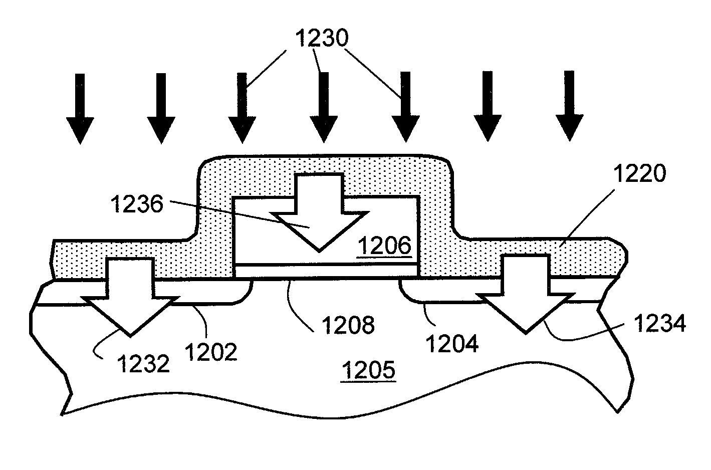
[0039]It is important to appreciate that concerns with respect to non-uniformity across the wafer surface in the thermal processing of semiconductor wafers are especially important in sensitive processing steps such as the annealing of ion implantation damage and the electrical activation of implanted dopant species. For instance, such processes are vital in the formation of source and drain regions of advanced transistors. These processes m...


PUM


Abstract

A method that is performed for heat treating a semiconductor wafer in a process chamber, as an intermediate part of an overall multi-step technique for processing the wafer, includes applying an energy transfer layer to at least a portion of the wafer, and exposing the wafer to an energy source in the process chamber in a way which subjects the wafer to a thermal profile such that the energy transfer layer influences at least one part of the thermal profile. The thermal profile has at least a first elevated temperature event. The method further includes, in time relation to the thermal profile, removing the energy transfer layer in the process chamber at least sufficiently for subjecting the wafer to a subsequent step. An associated intermediate condition of the wafer is described.

Description

BACKGROUND OF THE INVENTION[0001]The present invention relates generally to semiconductor processing systems and, more particularly, to a rapid thermal processing (RTP) system and method.[0002]During the manufacture of semiconductor devices, certain processes require the temporary heating of the surface of semiconductor wafers in order to, for example, promote annealing processes or other reactions that may be desired. Conventionally, this heating process, which is here referred to as rapid thermal processing (RTP), is performed by heating the wafer with some form of external energy source such as, for example, a bank of tungsten-halogen lamps or a hot-wall furnace.[0003]Recently, there has been renewed interest in very short heating cycles for processes such as annealing of ion-implantation damage for formation of ultra-shallow junctions. For example, a high temperature process may involve quickly heating a wafer to a peak temperature of approximately 1050° C. then immediately allo...

Claims


Application Information

Patent Timeline
Patent Type & Authority Patents(United States)
IPC IPC(8): H01L21/00
CPCH01L21/67115
Inventor TIMANS, PAUL J.
Owner MATTSON TECHNOLOGY
Why Eureka
Try Eureka