Semiconductor device and manufacturing method thereof

a technology applied in the field of semiconductor devices and manufacturing methods, can solve the problems of difficult manufacturing, inability to manufacture, and inability to work with micromachines, and achieve the effect of high manufacturing cost and high degree of freedom

Inactive Publication Date: 2010-01-05
SEMICON ENERGY LAB CO LTD
View PDF32 Cites 64 Cited by
  • Summary
  • Abstract
  • Description
  • Claims
  • Application Information

AI Technical Summary

Benefits of technology

[0017]The structural layer according to the present invention is obtained by laser crystallization or thermal crystallization using one or more of metal elements selected from Ni (nickel), Fe (iron), Ru (ruthenium), Rh (rhodium), Pd (palladium), Os (osmium), Ir (iridium), Pt (platinum), Cu (copper), and Au (gold). When crystallization is carried out using such a metal element, temperature at a crystallization step can be lowered; therefore, a substrate having a lower distortion point such as a glass substrate can be used.
[0043]According to the present invention, a semiconductor device in which a microstructure and a semiconductor element are formed over one substrate can be provided by using polycrystalline silicon obtained by crystallization using a metal element such as nickel for the structural layer of the microstructure and an active layer of the semiconductor element. Since the microstructure formed in this way can resist external force and stress, the microstructure can be formed over one substrate with the semiconductor element.
[0044]By manufacturing a microstructure and a semiconductor element over one substrate, a semiconductor device which does not require to be assembled and packaged and does not require high manufacturing cost can be provided.
[0045]Moreover, the present invention can provide a semiconductor device having a wireless communication circuit which enables control or power supply through wireless communication. Therefore, since the semiconductor device does not require wires for control or power supply to be connected to the semiconductor device, the semiconductor device can operate physically independently and have high degree of freedom. Thus, the provision of a central processing arithmetic circuit and the like for controlling the microstructure makes it possible to provide a semiconductor device which carries out a sequence of operations: detection, judgment, and act only by wireless communication control.

Problems solved by technology

It has been difficult to manufacture, by equivalent processes, a microstructure and a semiconductor element that form the above micromachine.
In this way, since different processes are necessary, there is a risk that the microstructure or semiconductor element may be broken so that the micromachine does not work.

Method used


Image

  • Semiconductor device and manufacturing method thereof
  • Semiconductor device and manufacturing method thereof
  • Semiconductor device and manufacturing method thereof

Examples


embodiment mode 1

[0065]Embodiment Mode 1 will describe a semiconductor device of the present invention with reference to the drawings.

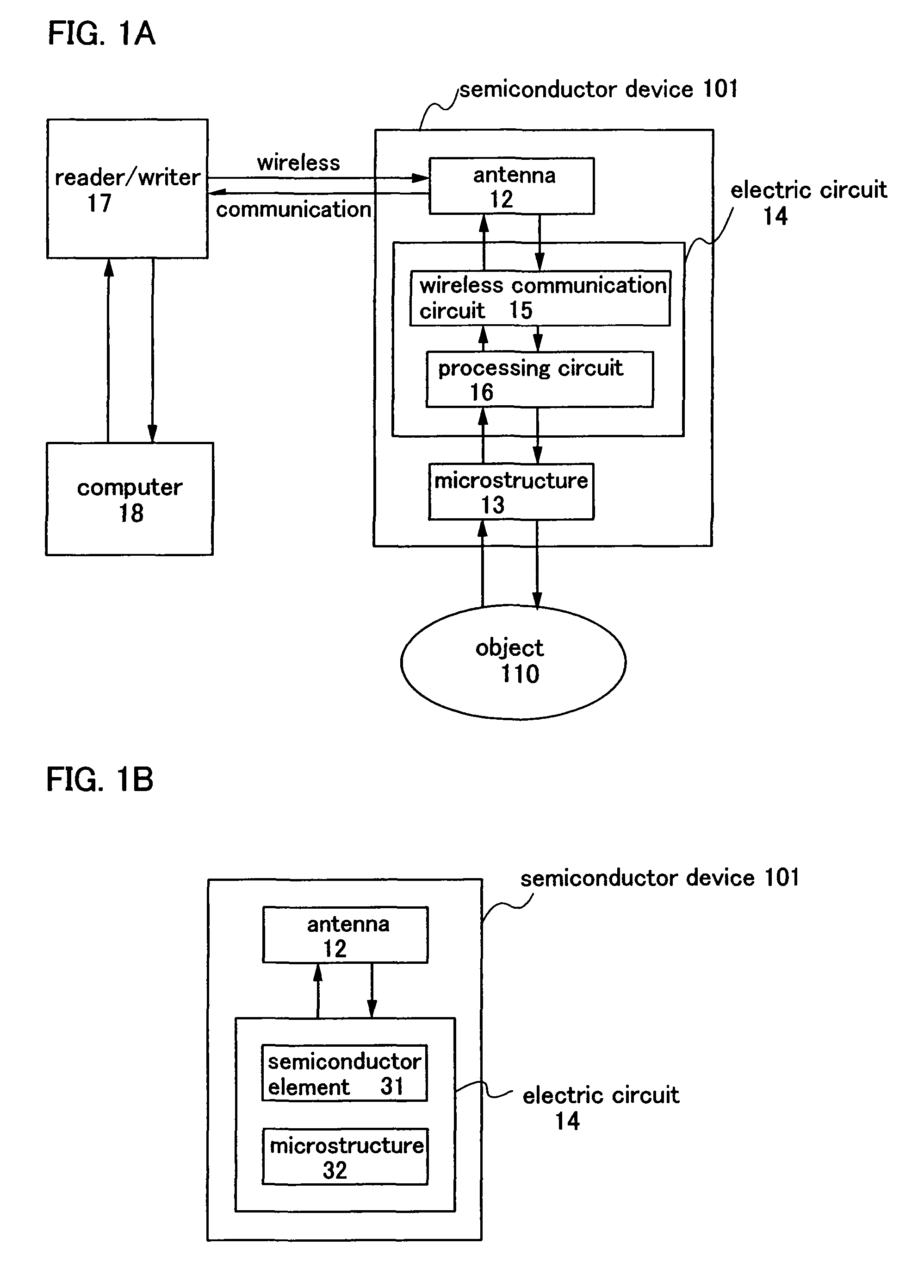
[0066]A semiconductor device of the present invention can control identification information using wireless communication. In other words, a semiconductor device of the present invention is provided with a wireless chip capable of controlling identification information using wireless communication. A semiconductor device provided with a wireless chip can carry out wireless communication with a reader / writer by obtaining drive electric power through an electromagnetic wave emitted from the reader / writer. Therefore, the semiconductor device of the present invention can be of nonbattery type. However, the semiconductor device of the present invention may have a battery or the like mounted in order to make up for drive electric power.

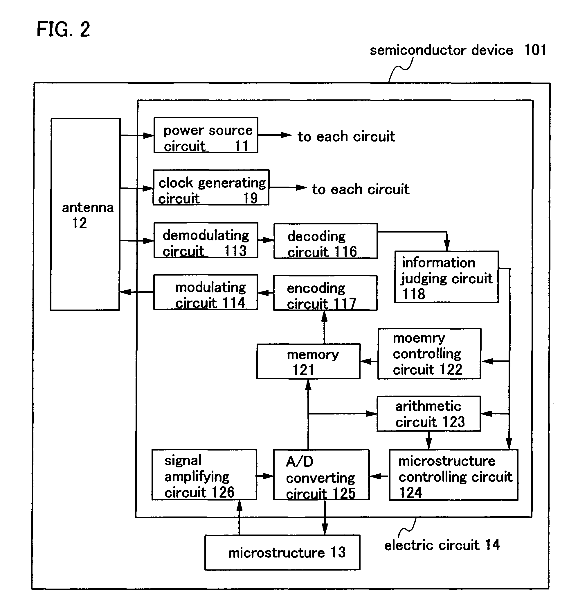
[0067]FIG. 1A shows a structure of a semiconductor device of the present invention. A semiconductor device 101 of the present invention incl...

embodiment mode 2

[0088]A microstructure provided in a semiconductor device of the present invention has different shape and structure depending on a function of the semiconductor device. This embodiment mode will describe a case where the microstructure functions as a sensor, an actuator, or a switch.

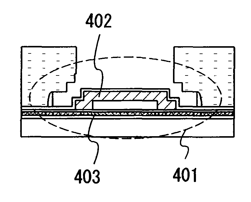
[0089]For example, a sensor can detect concentration, pressure, flow rate, or the like of an object. As an example of a typical structure of a microstructure having a function as a sensor, as shown in FIG. 3A, a microstructure 401 in which a structural layer 402 is provided over a substrate and a space is provided between the substrate and the structural layer 402 is given. When force is applied from outside to the microstructure having such a structure, the structural layer is deformed to change capacitance held between a lower layer and the structural layer. By detecting the change of the capacitance, applied force can be measured. The amount of change of the capacitance can be known by measuring pote...

embodiment mode 3

[0097]This embodiment mode will describe an example of using a microstructure for a wireless communication circuit.

[0098]In order to carry out wireless communication, the wireless communication circuit has a passive element such as an inductor or a capacitor and an active element such as a switch, in addition to a semiconductor element typified by a transistor. These elements can be manufactured in accordance with a technique for manufacturing a semiconductor element; however, some problems are caused. For example, the transistor used as a switch element has problems that difference in input voltage at ON state and OFF state cannot be increased, response speed cannot be raised, and so on.

[0099]However, it is considered that these problems can be solved by manufacturing these elements with the use of microstructures. For example, a switch manufactured by using a microstructure can completely insulate a signal transmission route at OFF state. Moreover, a control electrode of the switc...


PUM

PropertyMeasurementUnit
thicknessaaaaaaaaaa
thicknessaaaaaaaaaa
thicknessaaaaaaaaaa

Abstract

It has been difficult to manufacture a semiconductor device equipped with a microstructure having a space, an electric circuit for controlling the microstructure, and the like over one substrate.In a semiconductor device, a microstructure and an electric circuit for controlling the microstructure can be provided over one substrate by manufacturing the microstructure in such a way that a structural layer having polycrystalline silicon obtained by laser crystallization or thermal crystallization using a metal element is formed and processed at low temperature. As the electric circuit, a wireless communication circuit for carrying out wireless communication with an antenna is given.

Description

BACKGROUND OF THE INVENTION[0001]1. Field of Invention[0002]The present invention relates to a semiconductor device which has a microstructure and a semiconductor integrated circuit over one substrate and which communicates with outside wirelessly. Moreover, the present invention relates to a method for manufacturing the semiconductor device.[0003]2. Description of the Related Art[0004]In recent years, research has been advanced on a micromachine system called MEMS. MEMS stands for Micro Electro Mechanical System, and this is sometimes called a micromachine, simply. A micromachine generally indicates a microdevice in which “a movable microstructure having a three-dimensional structure” and “an electric circuit having a semiconductor element” are integrated by using a semiconductor microprocessing technique. Unlike a semiconductor element, the microstructure has a movable part and a three-dimensional structure. Moreover, the microstructure can have a function of a switch, a variable ...

Claims


Application Information

Patent Timeline
Patent Type & Authority Patents(United States)
IPC IPC(8): H01L29/82H01L23/58
CPCB81C1/00246H01L27/1214H01L27/1266H01L27/13B81C2203/0728H01L27/1255H01L27/1277
Inventor IZUMI, KONAMIYAMAGUCHI, MAYUMI
Owner SEMICON ENERGY LAB CO LTD
Why Eureka
Try Eureka