

Semiconductor device
a semiconductor and high-breakdown voltage technology, applied in the direction of semiconductor devices, basic electric elements, electrical appliances, etc., can solve the problems of increasing the the disadvantage of the sic power device in the cost, and the high cost of the sic power devi
- Summary
- Abstract
- Description
- Claims
- Application Information
AI Technical Summary
Benefits of technology
Problems solved by technology
Method used
Image

Examples
first embodiment
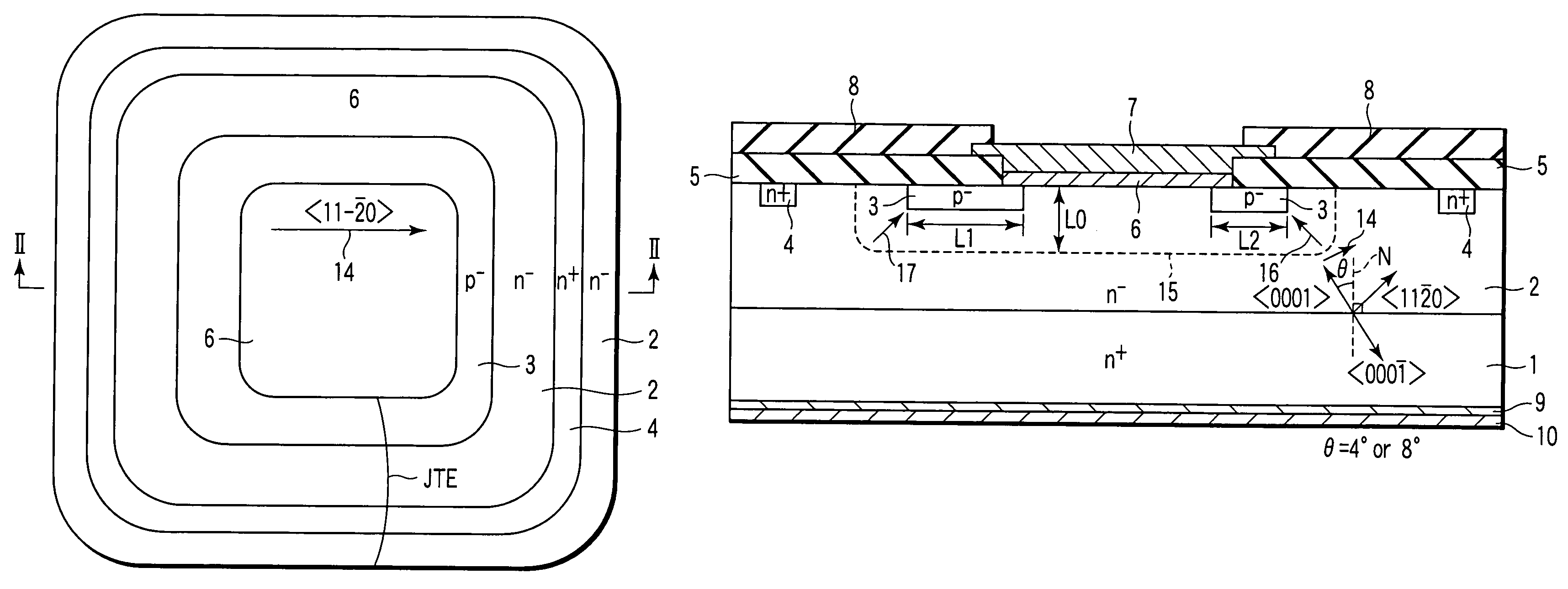
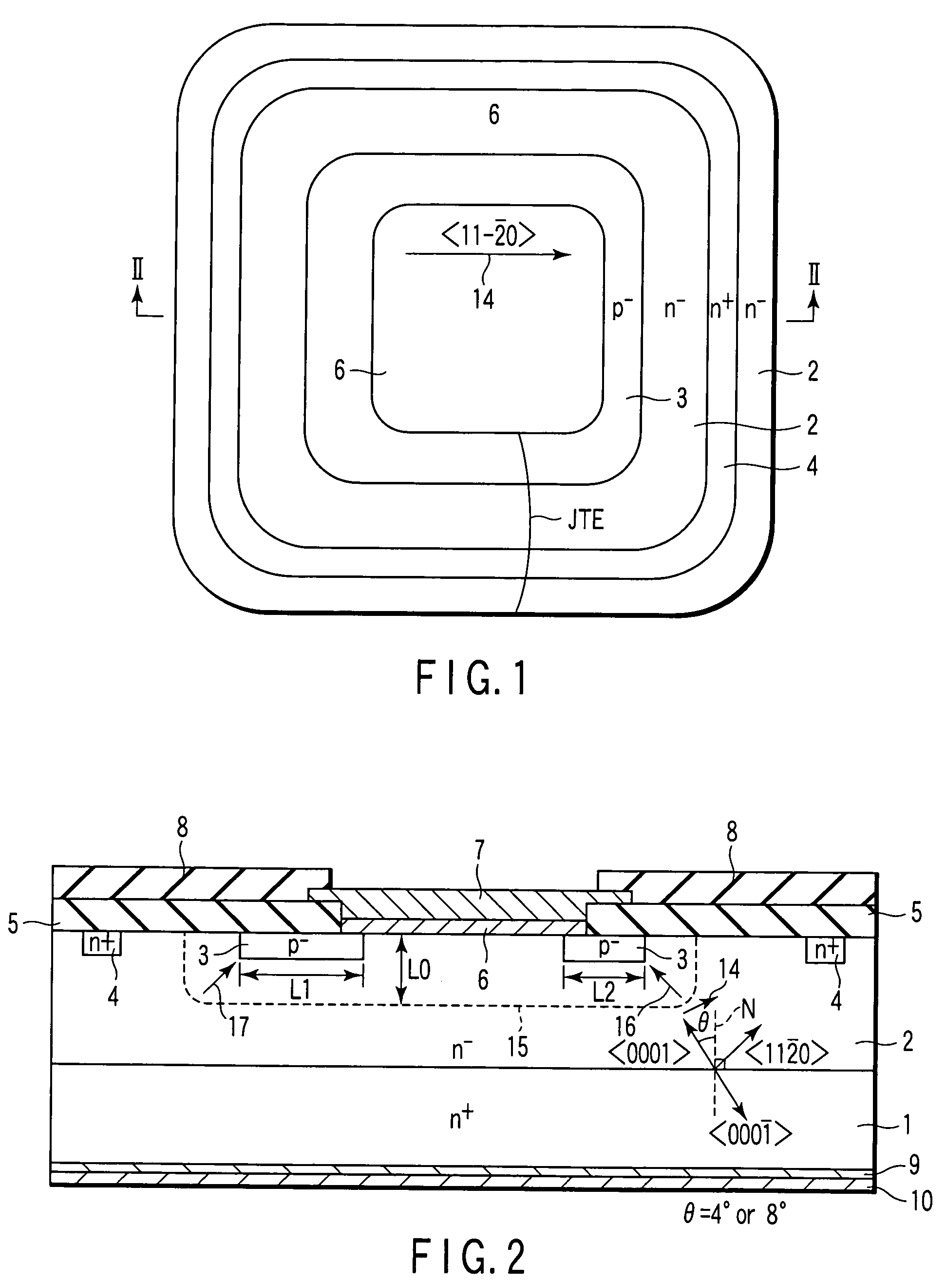
[0045]FIG. 1 is a plan view showing a high-breakdown-voltage semiconductor device according to a first embodiment of the present invention. FIG. 2 is a sectional view along a line II-II of FIG. 1. The high-breakdown-voltage semiconductor device of the present embodiment is provided with: a junction forming region in which an SiC Schottky diode is formed as an SiC power device; and a junction termination region including a RESURF region and a channel stopper region as junction termination structures.
[0046]In FIGS. 1 and 2, reference numeral 1 denotes an n-type SiC substrate having a high impurity concentration, and an n-type SiC layer 2 having a low impurity concentration is disposed on the surface of the n-type SiC substrate 1. The n-type SiC layer 2 is formed by an epitaxial growth process. That is, the layer is an epitaxially grown layer.
[0047]A main surface of the n-type SiC substrate 1 is provided with a normal N tilted (being off) at a predetermined off angle of usually 4° or 8...
second embodiment
[0072]FIG. 5 is a plan view showing a high-breakdown-voltage semiconductor device according to a second embodiment of the present invention. FIG. 6 is a sectional view along a line VI-VI of FIG. 5. It is to be noted that in the figures, components corresponding to those of the first embodiment are denoted with the same reference numerals, and detailed description thereof is omitted.
[0073]The present embodiment is different from the first embodiment in that a power MOSFET is used instead of a Schottky diode. The present embodiment is provided with a RESURF region similar to that of the first embodiment, and for a reason similar to that of the first embodiment, different electric field intensities are applied to the layer on upstream and downstream sides of an off direction.
[0074]As shown in FIG. 6, p-type wells 21 are selectively formed in the surface of an n-type SiC layer 2, and n-type source layers 22 are selectively formed in the surfaces of the p-type wells 21. Each gate electro...
third embodiment
[0076]FIG. 7 is a sectional view showing the high-breakdown-voltage semiconductor device according to a third embodiment of the present invention. The present embodiment is different from the first embodiment in that an IGBT is used instead of a Schottky diode.
[0077]Basically, the n-type SiC substrate 1 of the second embodiment is replaced with a p-type SiC substrate 1′ to constitute the IGBT of the present embodiment. Instead of simply replacing the n-type SiC substrate 1 with the p-type SiC substrate 1′, the substrate may be replaced with a substrate including an n-type SiC layer disposed on a p-type SiC layer, each having a high impurity concentration.
[0078]Also in the present embodiment, in the same manner as in the second embodiment, widths of a RESURF region 5 on upstream and downstream sides of an off direction are set to values in accordance with an electric field reducing effect, and unnecessary junction termination regions are reduced. Consequently, costs can be reduced wh...
PUM
 Abstract
Description
Claims
Application Information