Structures for Z-aligned proximity communication

a technology of proximity communication and structure, applied in the direction of semiconductor devices, semiconductor/solid-state device details, electrical apparatus, etc., can solve the problems of destroying received signals, affecting the smooth operation of the chip, and the inability to properly align the chips using existing mounting structures, etc., to achieve greater flexibility compliance, reduce misalignment, and reduce misalignment

Active Publication Date: 2010-02-09
ORACLE INT CORP
View PDF6 Cites 6 Cited by
  • Summary
  • Abstract
  • Description
  • Claims
  • Application Information

AI Technical Summary

Benefits of technology

[0023]In some embodiments, the system further includes a control circuit. The control circuit provides feedback to reduce misalignment in the first direction between the first plurality of proximity connectors and the second plurality of proximity connectors.
[0024]In some embodiments, the first semiconductor die is configured to have a flexibility compliance greater than a third pre-determined value in the first direction in order to reduce misalignment in the first direction between the first plurality of proximity connectors and the second plurality of proximity connectors.
[0025]In some embodiments, the system further includes a second semiconductor die having a fifth surface and a sixth surface. The second semiconductor die is configured to communicate by capacitive coupling using one or more of a third plurality of proximity connector

Problems solved by technology

Misalignment in the plane may cause each receiving pad to span two transmitting pads, thereby destroying a received signal.
Unfortunately, it is not a simple matter to align the chips properly using existing mounting structures, such as conventional single-chip modules or conventional multi-chip modules.
The chips in these structures are subje

Method used


Image

  • Structures for Z-aligned proximity communication
  • Structures for Z-aligned proximity communication
  • Structures for Z-aligned proximity communication

Examples


embodiment 200

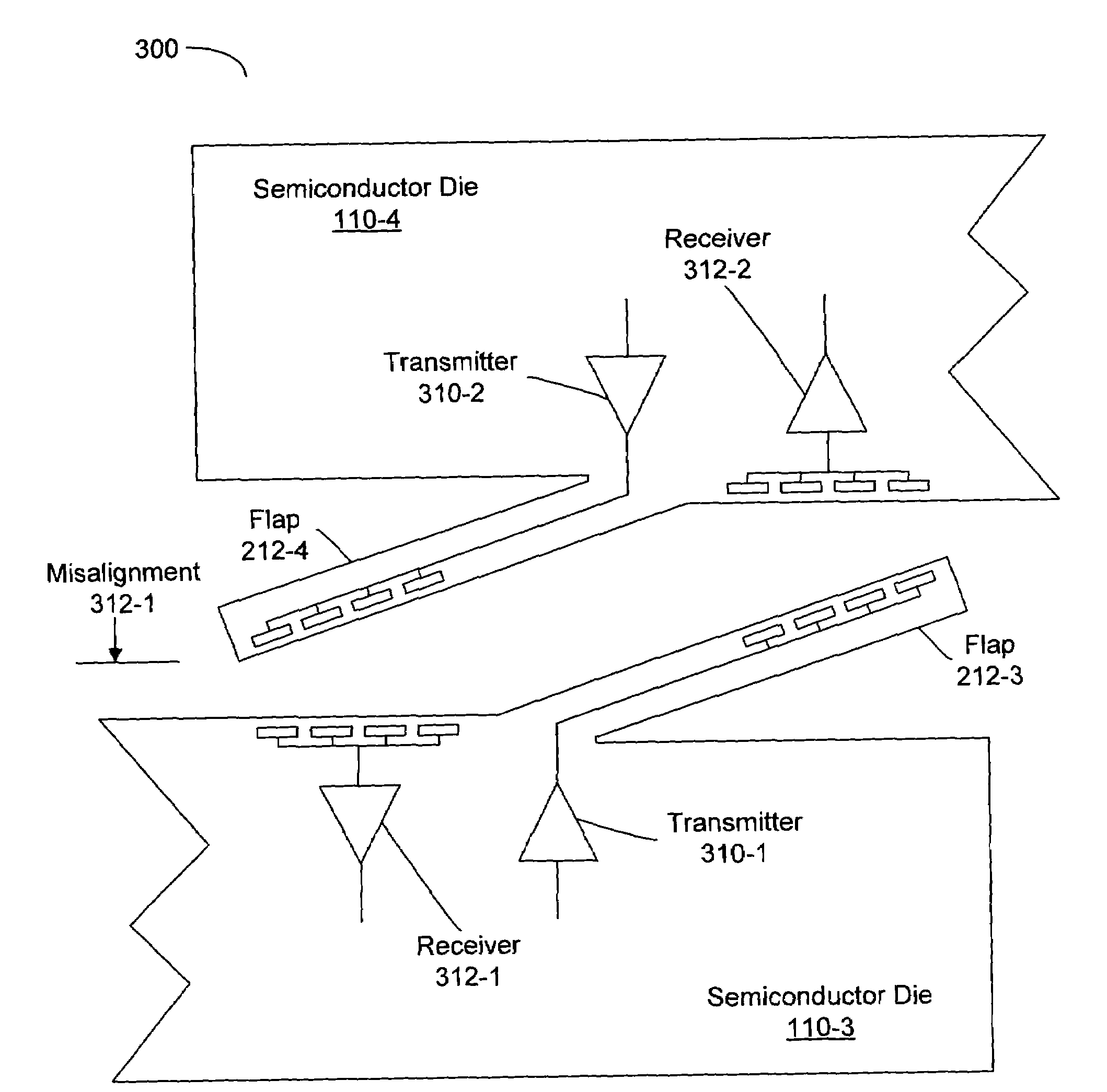
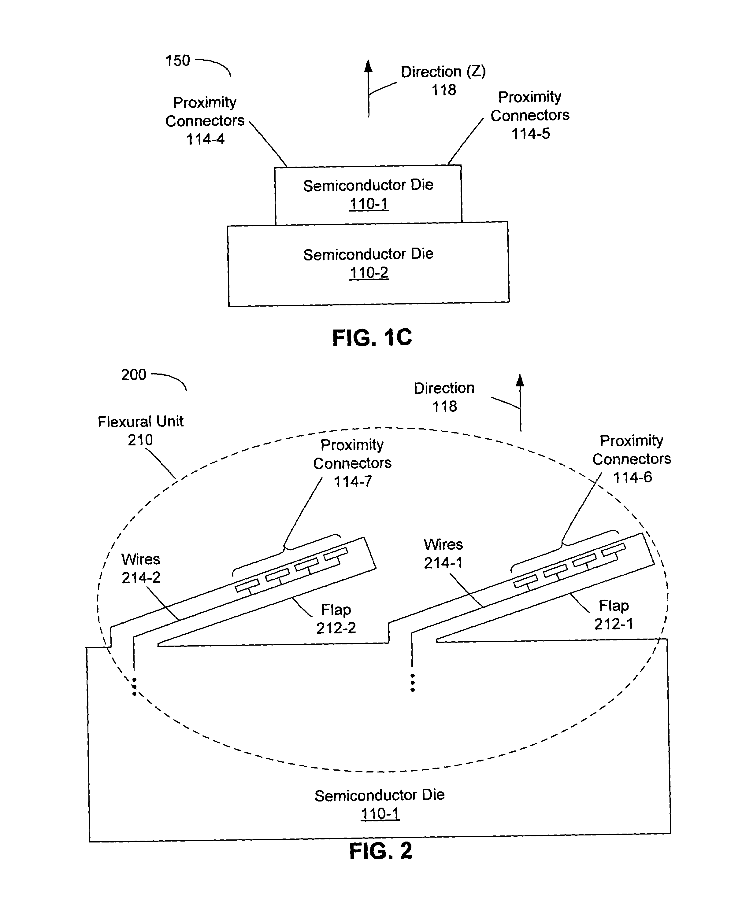
[0065]FIG. 2 is a block diagram illustrating a side view of an embodiment 200 of the semiconductor die 110-1 having a flexural unit 210. The flexural unit 210 may include one or more flaps 212. The flaps 212 are intentionally non-adherent to a portion of a surface of the semiconductor die 110-1. This may be accomplished using micro electro-mechanical system (MEMS) techniques that are known in the art to remove material beneath the flaps 212 (for example, using a sacrificial layer). The flaps 212, including wires 214 and proximity connectors 114 (each including one or more pads or connectors), have a flexibility compliance greater than the pre-determined value in the third direction (Z) 118. This flexibility allows the flaps 212 to displace approximately along the third direction (Z) 118 and relative to a centroid of the semiconductor die 110-1.

[0066]The flaps 212 may have a variety of cross-sectional shapes including rectangular and square. When viewed from above (such as the top vi...

embodiment 700

[0081]This approach is illustrated in FIG. 7, which is a block diagram showing a side view of an embodiment 700 of a semiconductor die 110-11 having at least one electromechanical transducer 710. The electromechanical transducer 710 provides a mating force. The electro-mechanical transducer 710 is closely coupled to a structure having a flexibility compliance, such as flap 212-8. An optional control circuit 712 may be included as part of a feedback loop based on a misalignment sensor (not shown).

[0082]The optional control circuit 712 may compare a measured misalignment, such as the misalignment 312-3 (FIG. 4), with a desired misalignment (i.e., a desired gap) between adjacent semiconductor dies. The optional control circuit 712 in the feedback loop may reduced and / or eliminate the misalignment even when there are considerable perturbations due to fabrication, assembly, operation and / or external causes, by providing control signals to the electromechanical transducer 710.

[0083]In som...


PUM


Abstract

A device includes a first semiconductor die having a first surface and a second surface. The first semiconductor die is configured to communicate by capacitive coupling using one or more of a plurality of proximity connectors proximate to the first surface. The first semiconductor die is configured to have a flexibility compliance greater than a first pre-determined value in a direction substantially perpendicular to a plane including the plurality of proximity connectors in order to reduce misalignment in the direction between the plurality of proximity connectors and additional proximity connectors on another device.

Description

CROSS REFERENCE TO RELATED APPLICATIONS[0001]This application claims priority under 35 U.S.C. 119(e) to U.S. Provisional Application Ser. No. 60 / 618,646, filed on Oct. 13, 2004, the contents of which are herein incorporated by reference.GOVERNMENT LICENSE RIGHTS[0002]This invention was made with United States Government support under Contract No. NBCH3039002 awarded by the Defense Advanced Research Projects Administration. The United States Government has certain rights in the invention.BACKGROUND[0003]1. Field of the Invention[0004]The present invention relates to connector alignment for semiconductor dies. More specifically, the present invention relates to structures having flexibility compliance to facilitate communication of signals between semiconductor dies using proximity connectors.[0005]2. Related Art[0006]Researchers have begun to investigate alternative techniques for communicating between semiconductor chips. One promising technique involves integrating arrays of capaci...

Claims


Application Information

Patent Timeline
IPC IPC(8): H01L29/41
CPCH01L23/48H01L2924/14H01L2924/30105H01L2924/3011H01L2924/0002H01L2924/00
Inventor ZINGHER, ARTHUR R.MOFFAT, ROBERT J.HO, RONALD
Owner ORACLE INT CORP
Why Eureka
Try Eureka