Semiconductor device including fuse focus detector, fabricating method thereof and laser repair method using the fuse focus detector

a technology of fuse focus and laser repair method, which is applied in the direction of solid-state devices, basic electric elements, manufacturing tools, etc., can solve the problems affecting the uniformity of the final thickness of the fuse in different regions of the wafer, and affecting the quality of the final thickness of the fuse, etc., to achieve the effect of reducing the rate of generating defective semiconductor devices during the laser repair process

Inactive Publication Date: 2010-03-02
SAMSUNG ELECTRONICS CO LTD
View PDF9 Cites 3 Cited by
  • Summary
  • Abstract
  • Description
  • Claims
  • Application Information

AI Technical Summary

Benefits of technology

[0009]An example embodiment of the present invention also provides a method of fabricating a semiconductor device. The method may perform a fuse cutting operation based on an appropriate focus offset value depending on a position on a wafer by forming a fuse focus detector through a relatively simple process without securing additional space in a chip region.
[0010]An example embodiment of the present invention also provides a laser repair method. The laser repair method may reduce a defect generation rate by determining an appropriate focus offset value of a laser beam with considering a variation in the thickness of fuses depending on a position of the fuses on a wafer.
[0020]According to the example embodiments of the present invention, because the fuse focus detector may be formed in the scribe line region, securing additional space in the chip region of a highly integrated semiconductor device may not be necessary. Also, an additional process of forming the fuse focus detector may not be necessary. Even if the fuses formed at the same level on the wafer have different thickness depending on a position of the fuses on the wafer, an accurate focus offset value for the fuse to be cut may be calculated, and the fuse cutting may be performed if the calculated focus offset value is within an allowable range. Accordingly, a rate of generating defective semiconductor devices during the laser repair process may be reduced according to example embodiments of the present invention.

Problems solved by technology

As semiconductor devices are becoming highly integrated and a capacitance level thereof is also being increased, memory cells are more likely to have defects resulting from the fabrication of the semiconductor devices.
However, when an etching process is performed to open the fuses during a method of fabricating a semiconductor device, the fuses may be exposed and may have varying thickness from the top.
Therefore, it may be difficult to control the uniformity of the final thicknesses of the fuses in different regions of the wafer.
As a result, fuses adjacent to a target fuse to be cut may be damaged and / or the target fuse may not be cut.
Also, because a difference between focus offset values of a central region and an edge region may be large, a number of chips on a wafer may be severely affected and / or become defective.

Method used


Image

  • Semiconductor device including fuse focus detector, fabricating method thereof and laser repair method using the fuse focus detector
  • Semiconductor device including fuse focus detector, fabricating method thereof and laser repair method using the fuse focus detector
  • Semiconductor device including fuse focus detector, fabricating method thereof and laser repair method using the fuse focus detector

Examples


Embodiment Construction

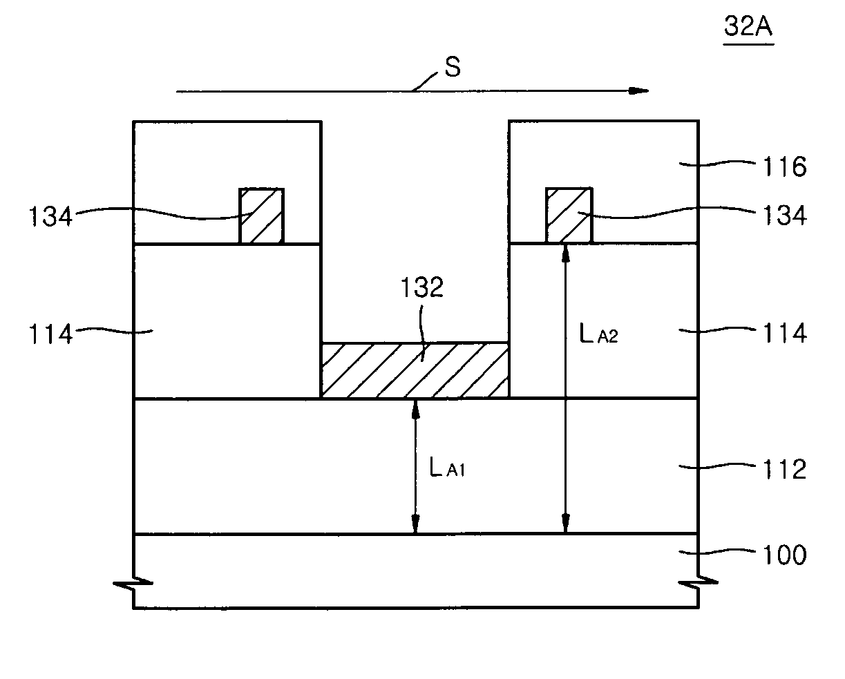
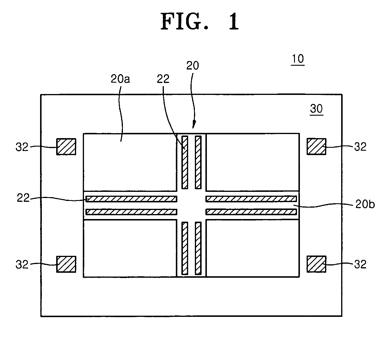
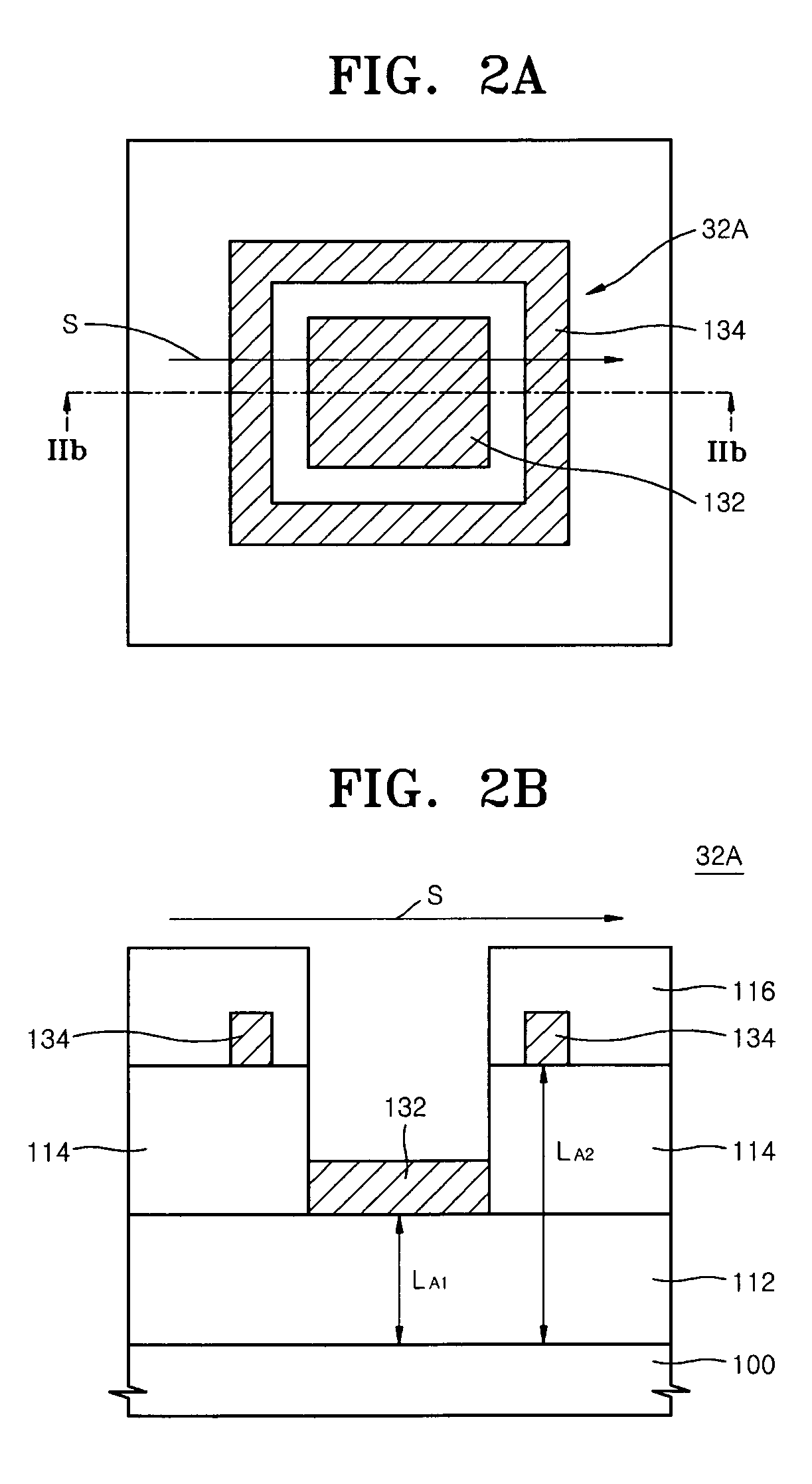
[0032]Detailed illustrative embodiments of the present invention are disclosed herein. However, specific structural and functional details disclosed herein are merely representative for purposes of describing example embodiments of the present invention. This invention may, however, be embodied in many alternate forms and should not be construed as limited to only the embodiments set forth herein.

[0033]Accordingly, while example embodiments of the present invention are capable of various modifications and alternative forms, embodiments of the present invention are shown by way of example in the drawings and will herein be described in detail. It should be understood, however, that there is no intent to limit example embodiments of the invention to the particular forms disclosed, but on the contrary, example embodiments of the invention are to cover all modifications, equivalents, and alternatives falling within the scope of the invention.

[0034]It should also be understood that, alth...


PUM

PropertyMeasurementUnit
heightaaaaaaaaaa
conductiveaaaaaaaaaa
shapeaaaaaaaaaa

Abstract

Provided are a semiconductor device including a fuse focus detector, a fabrication method thereof and a laser repair method. In a chip region, fuses may be formed at a first level. A fuse focus detector including first and second conductive layers may be formed in a scribe line region. The first conductive layer may be formed at the first level, while the second conductive layer may be formed at a different level. For a laser repair method, a target region may be divided into sub-regions. In one selected sub-region, the fuse focus detector may be laser scanned in a direction for a reflection light measurement providing information on a thickness of the fuse focus detector. Using the thickness information, a focus offset value of a fuse in the selected sub-region may be calculated. When the focus offset value is within an allowable range, fuse cutting may be performed.

Description

PRIORITY STATEMENT[0001]This application claims the benefit of priority to Korean Patent Application No. 10-2005-0116641, filed on Dec. 1, 2005, in the Korean Intellectual Property Office, the entire contents of which are incorporated herein by reference.BACKGROUND OF THE INVENTION[0002]1. Field of the Invention[0003]Example embodiments of the present invention relate to a semiconductor device including a fuse coupled with a redundancy circuit, a fabrication method thereof and a laser repair method for a semiconductor device using fuse cutting. More particularly, example embodiments of the present invention relate to a semiconductor device including a fuse focus detector for determining a focus offset value of a laser beam used for laser cutting, a semiconductor device fabrication method and a laser repair method using the fuse focus detector.[0004]2. Description of the Related Art[0005]As semiconductor devices are becoming highly integrated and a capacitance level thereof is also b...

Claims


Application Information

Patent Timeline
Patent Type & Authority Patents(United States)
IPC IPC(8): H01L23/58
CPCB23K26/0003H01L23/5258H01L23/544H01L2223/5446H01L2924/0002B23K26/351H01L2924/00H01L21/82
Inventor BANG, KWANG-KYULEE, YONG-WONSHIN, KYEONG-SEONJU, HYEN-WOOKKIM, JEONG-KYU
Owner SAMSUNG ELECTRONICS CO LTD
Why Eureka
Try Eureka