Empty vias for electromigration during electronic-fuse re-programming
a technology of electronic fuse and via, applied in the field of integrated circuit (ic) chip fabrication, can solve the problems of major reliability concerns and difficulty in circuit programming at the product level after packaging
- Summary
- Abstract
- Description
- Claims
- Application Information
AI Technical Summary
Benefits of technology
Problems solved by technology
Method used
Image
Examples
Embodiment Construction
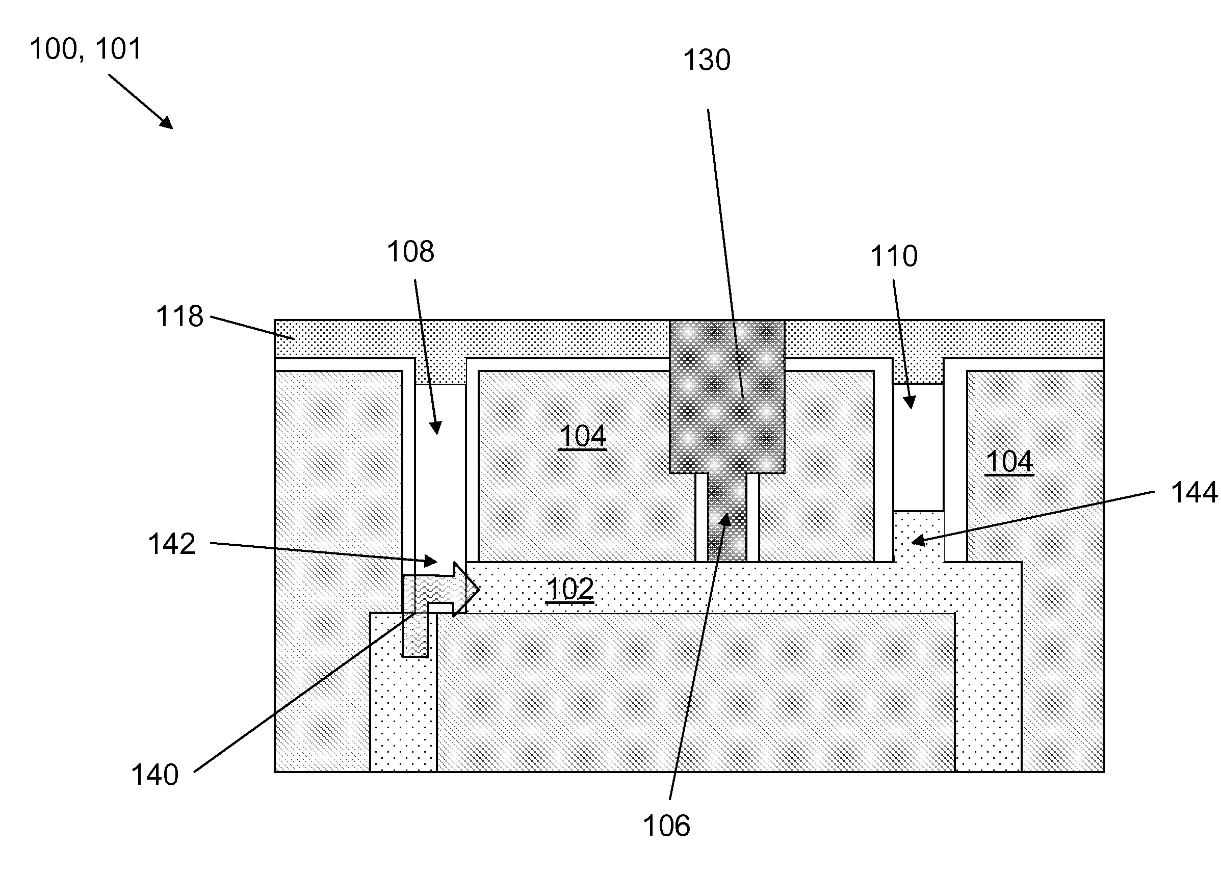
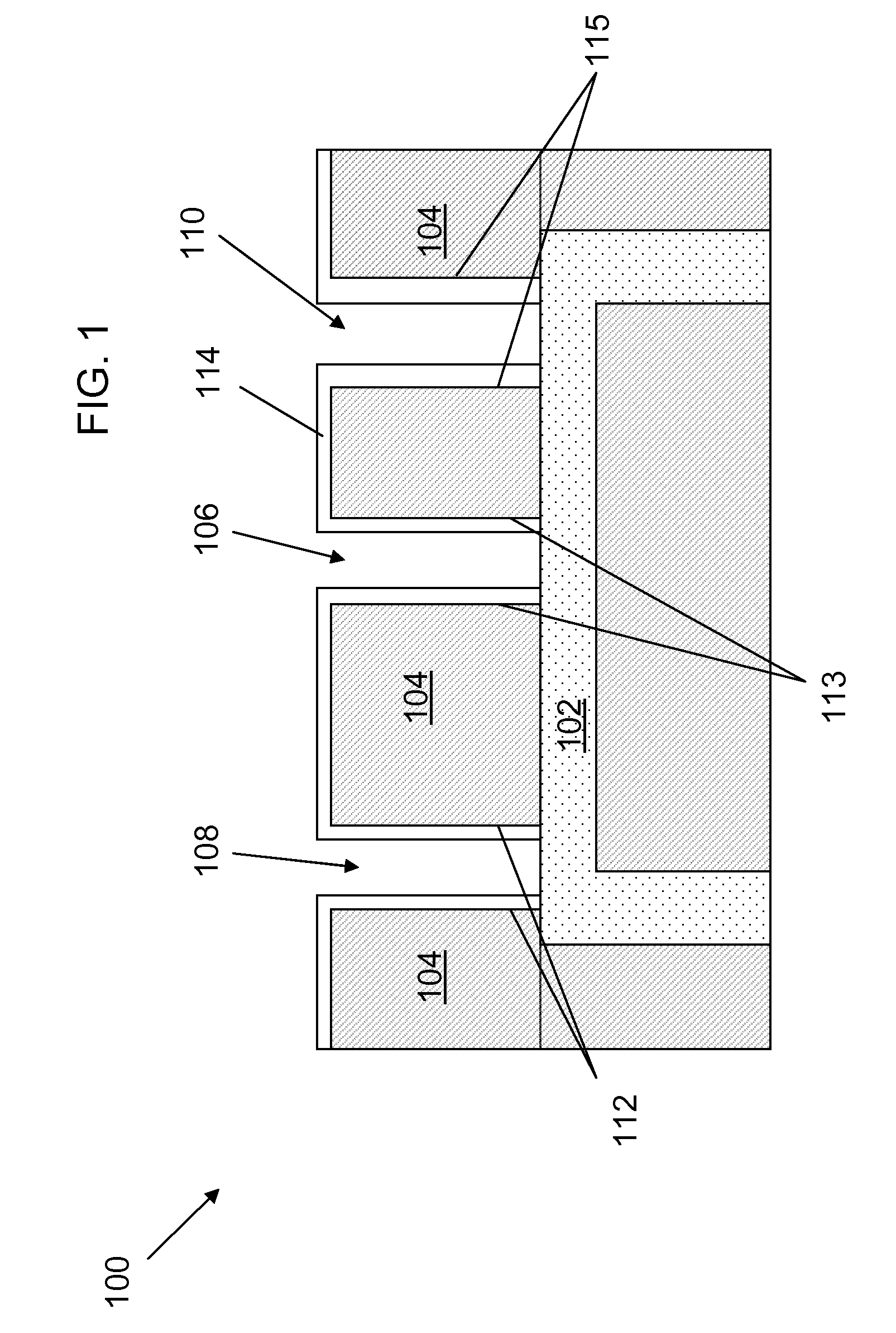
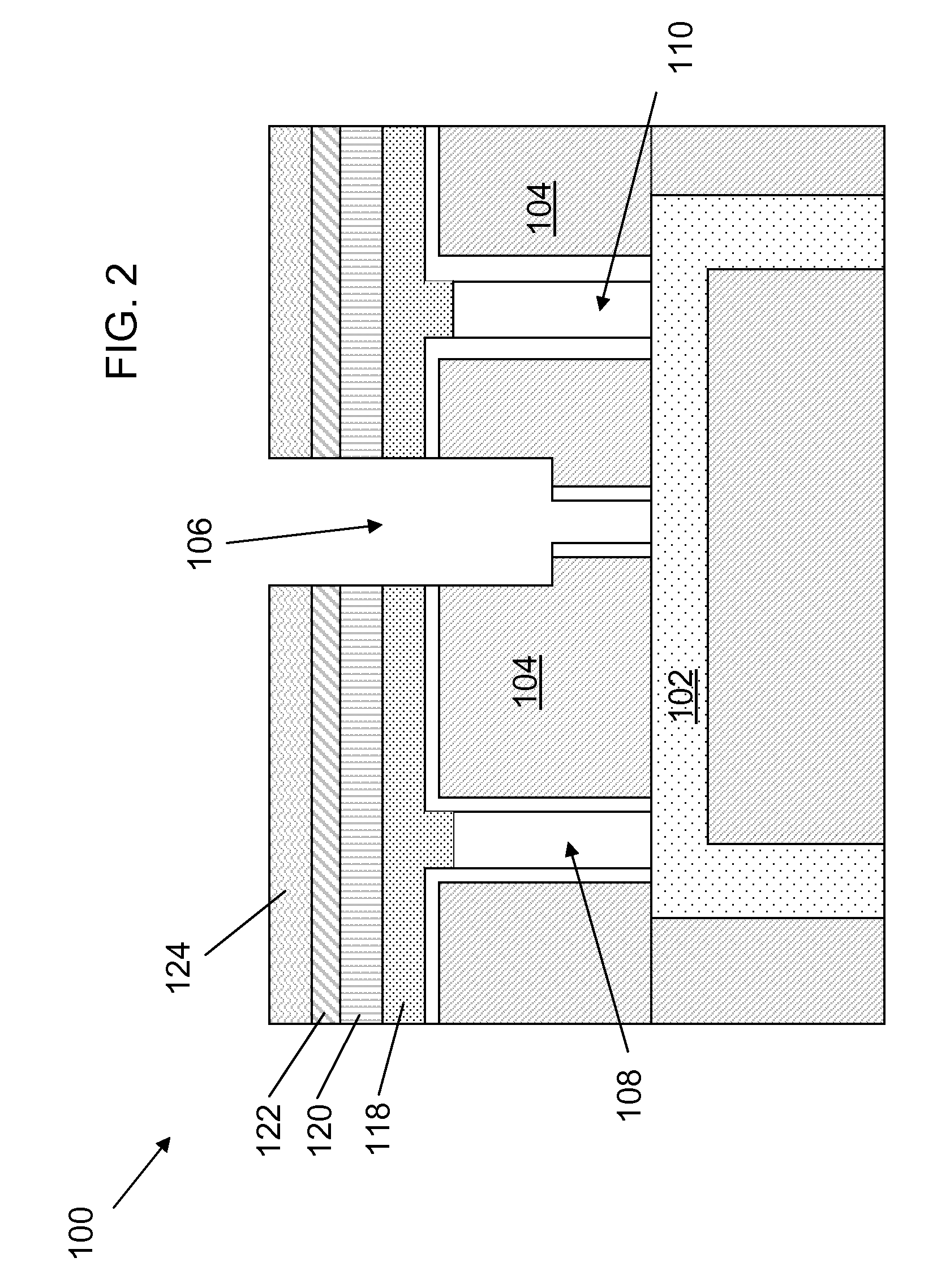
[0012]Turning to the drawings, FIG. 1 shows a preliminary structure 100, to which methods according to embodiments of the disclosure will be applied. Although a single structure 100 is shown for the sake of clarity, it should be appreciated that multiple structures are possible. As shown, an interlayer dielectric 104 may be formed over an interconnect 102 to form an electrical fuse (e-fuse) device. Interconnect 102 includes any one of a number of materials selected from the group consisting of copper (Cu), aluminum (Al), copper-clad aluminum and silver (Ag). Interlayer dielectric 104 includes any of a number of materials, including a low or ultra low k (ULK) dielectric constant material comprising atoms of silicon, carbon, oxygen and hydrogen (SiCOH), silicon (Si), silicon dioxide (SiO2) and silicon nitride (Si3N4). As also shown in FIG. 1, an opening 106, a first via 108 and a second via 110 are formed in interlayer dielectric 104, wherein opening 106, first via 108 and second via ...
PUM
 Abstract
Description
Claims
Application Information


