Method and apparatus for nondestructively evaluating light-emitting materials

a light-emitting material and non-destructive technology, applied in the direction of individual semiconductor device testing, material analysis, instruments, etc., can solve the problems of unfulfilled need for non-destructive characterization, high photoluminescence efficiency, and still too expensive light-emitting technologies for wide-spread applications

Active Publication Date: 2010-03-16
MAXMILE TECH
View PDF10 Cites 13 Cited by
  • Summary
  • Abstract
  • Description
  • Claims
  • Application Information

AI Technical Summary

Benefits of technology

[0012]In accordance with yet another aspect of the present invention, an apparatus for evaluating the light-emitting material is disclosed. The apparatus is developed based on the disclosed LED / OLED probe. With a means for applying an electrical stimulus in the probe and a means for measuring the electroluminescence and electrical response, the electroluminescence and electrical properties of various regions in the light-emitting materials can be nondestructively and independently evaluated. The advantage of the present invention is that the corresponding evaluation can be done at the wafer level yet as the finished device (LED or OLED) functions through electroluminescence.
[0013]Preferably, the apparatus includes a translation means for relatively translating the LED / OLED probe and the test material. The translation stage can be controlled at wafer-level or micrometric scale. With a scanning stage, the above evaluations can be used to determine the wafer-level uniformity about light emission intensity, peak wavelength, wavelength variation, spectrum half width and electrical / optical energy conversion efficiencies, as well as electrical properties of different layers. The micrometric-scale scanning capability could be used for localized investigations such as defect influence on device performance.
[0014]Optionally, the apparatus includes a light injection means which can be used to characterize the photoluminescence. The photoluminescence will be measured by the same means for measuring the electroluminescence in the apparatus. The advantage of adding the option of photoluminescence measurement is that both photoluminescence and electroluminescence can be measured from the same sample location which can provide an extra dimension of information to evaluate the material.

Problems solved by technology

However, these lighting technologies are still too expensive for wide-spread applications.
High photoluminescence efficiency is necessary but not sufficient for a good light-emitting materials or wafers.
Thus, there remains an unfulfilled need for non-destructively characterizing the light-emitting materials which can be used for improved quality control at the wafer level.
The prior art also does not teach effective means for separating out the various factors attributed to a poor electroluminescence which could result from the failure at any layers of the material structure, or from the problem caused by device (LED / OLED) fabrication.
Though device fabrication and device level test could teach a mean to correlate the different factors with the device performance or the electroluminescence, such approach is expensive in terms of personnel time and material cost, and sometimes it still can be difficult or even impossible to trace failure factors.

Method used


Image

  • Method and apparatus for nondestructively evaluating light-emitting materials
  • Method and apparatus for nondestructively evaluating light-emitting materials
  • Method and apparatus for nondestructively evaluating light-emitting materials

Examples


Embodiment Construction

[0021]The present invention will be described with the reference to the accompanying figures wherein like reference numbers correspond to like elements.

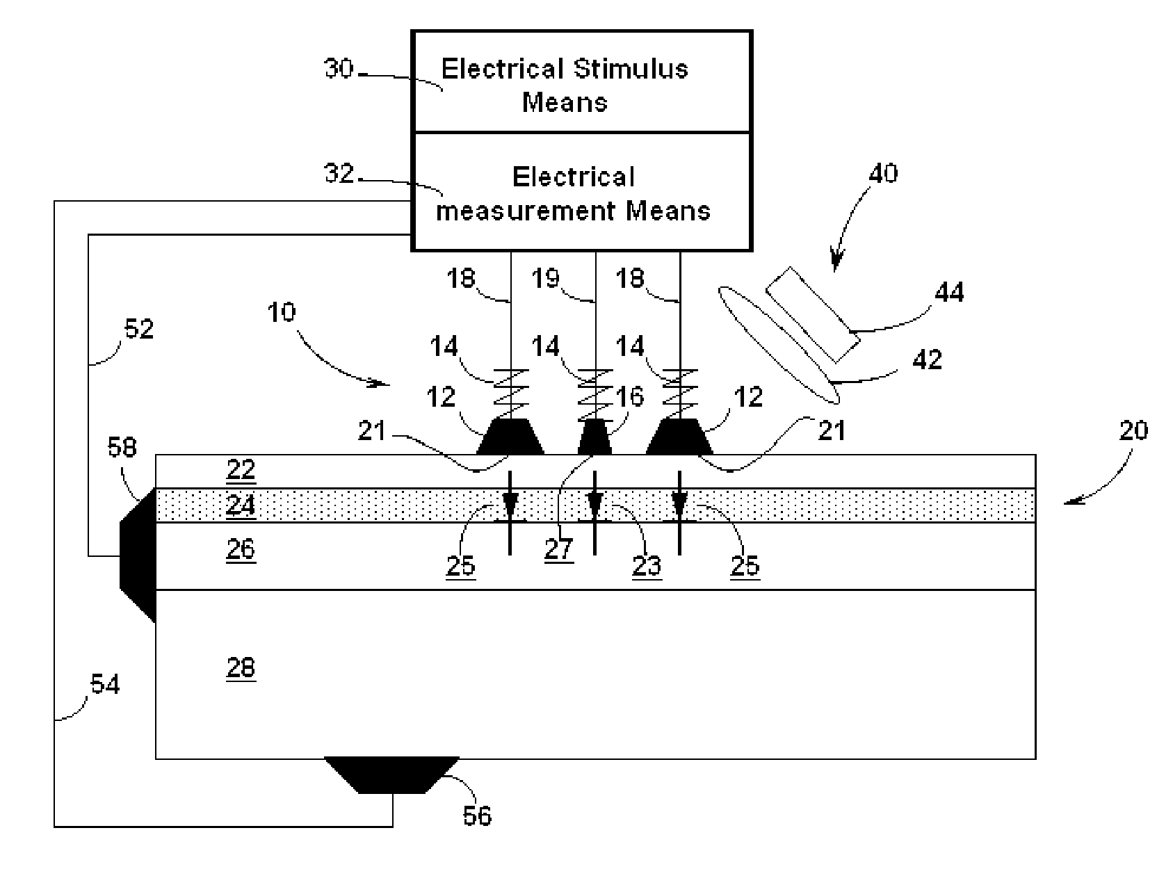
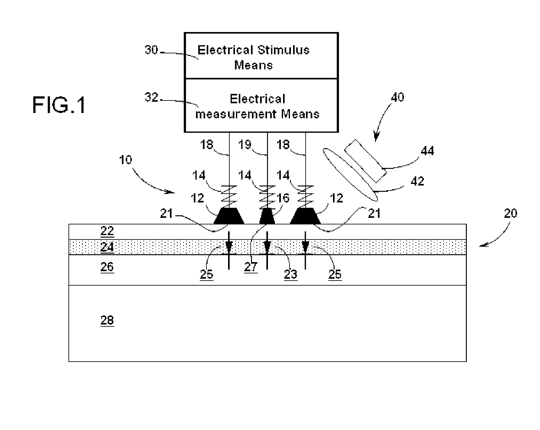
[0022]With reference to FIG. 1, a light-emitting material testing method is described in accordance with one embodiment of the nondestructive LED / OLED probe. The nondestructive LED / OLED probe 10 operates upon an associated light-emitting sample 20. The associated sample 20 typically has a plurality of layers 22, 24, 26 which are usually grown on a substrate 28. In FIG. 1, a gallium nitride (GaN) based LED structure is exemplarily shown, which includes a sapphire or silicon carbide (SiC) substrate 28, a p-type GaN region 22 and a n-type GaN region 26. The sandwiched layer between the p-type GaN region 22 and the n-type GaN 26 are AlInGaN (Al: aluminum, In: indium) multi-quantum-well barriers 24 which comprise the active / emissive region of LED device. Electrically the p-type GaN region 22 and the n-type GaN region 26 can be briefed as ...


PUM


Abstract

An evaluation apparatus is taught to nondestructively characterize the electroluminescence behavior of the semiconductor-based or organic small-molecule or polymer-based light-emitting material as the finished light-emitting device functions through electroluminescence. An electrode probe is used to temporarily form a light-emitting device through forming an intimate electrical contact to the surface of the light emitting material. A testing system is provided for applying an electrical stimulus to the electrode probe and temporarily formed device and for measuring the electrical and optical / electroluminescence response to the electrical stimulus. The electrical and optical properties of the light-emitting material can be nondestructively determined from the measured response. Optionally a light stimulus is used to perform the photoluminescence characterization together with the electroluminescence characterization, and both characterizations can be performed at the same sample location or / and at the wafer level.

Description

FIELD OF THE INVENTION[0001]This invention relates to light-emitting materials characterization or evaluation, and more specifically to the optical and electrical characterization of the electroluminescence materials which can be used for fabricating light-emitting diode (LED) or organic light-emitting diodes (OLED). Though the invention will be described with particular reference to the quantum well-based LED materials system, the invention is not so limited, and it will also find applications in optical, electrical and optoelectronic evaluation of all type light-emitting materials systems which are semiconductor-based or organic small-molecule or polymer-based, as well as p / n junction, semiconductor laser structures, and the like.DESCRIPTION OF RELATED ART[0002]Breakthroughs in artificial lighting from semiconductor-based or organic small-molecule- or polymer-based light-emitting materials system have led to tremendous opportunities in modern society. Solid-state lighting (SSL) ba...

Claims


Application Information

Patent Timeline
Patent Type & Authority Patents(United States)
IPC IPC(8): G01R31/02G01R31/26
CPCG01N21/6489G01N21/66G01N21/9505G01R31/2635G01R1/073
Inventor MA, XIANYUN
Owner MAXMILE TECH
Why Eureka
Try Eureka