
Capacitors with insulating layer having embedded dielectric rods

a dielectric rod and capacitor technology, applied in the field of decoupling capacitors, can solve the problems of inferior ability to suppress ssn, difficult to find and process such materials, and serious signal integrity and electromagnetic interference problems, and achieve the effect of improving high-frequency performance and increasing capacitan

Inactive Publication Date: 2010-03-16
TAIWAN SEMICON MFG CO LTD
View PDF9 Cites 44 Cited by
  • Summary
  • Abstract
  • Description
  • Claims
  • Application Information

AI Technical Summary

Benefits of technology

This configuration significantly increases capacitance per unit area and improves high-frequency performance by reducing noise and electromagnetic interference, offering adjustable central frequency and bandwidth through the arrangement of dielectric rods.

Problems solved by technology

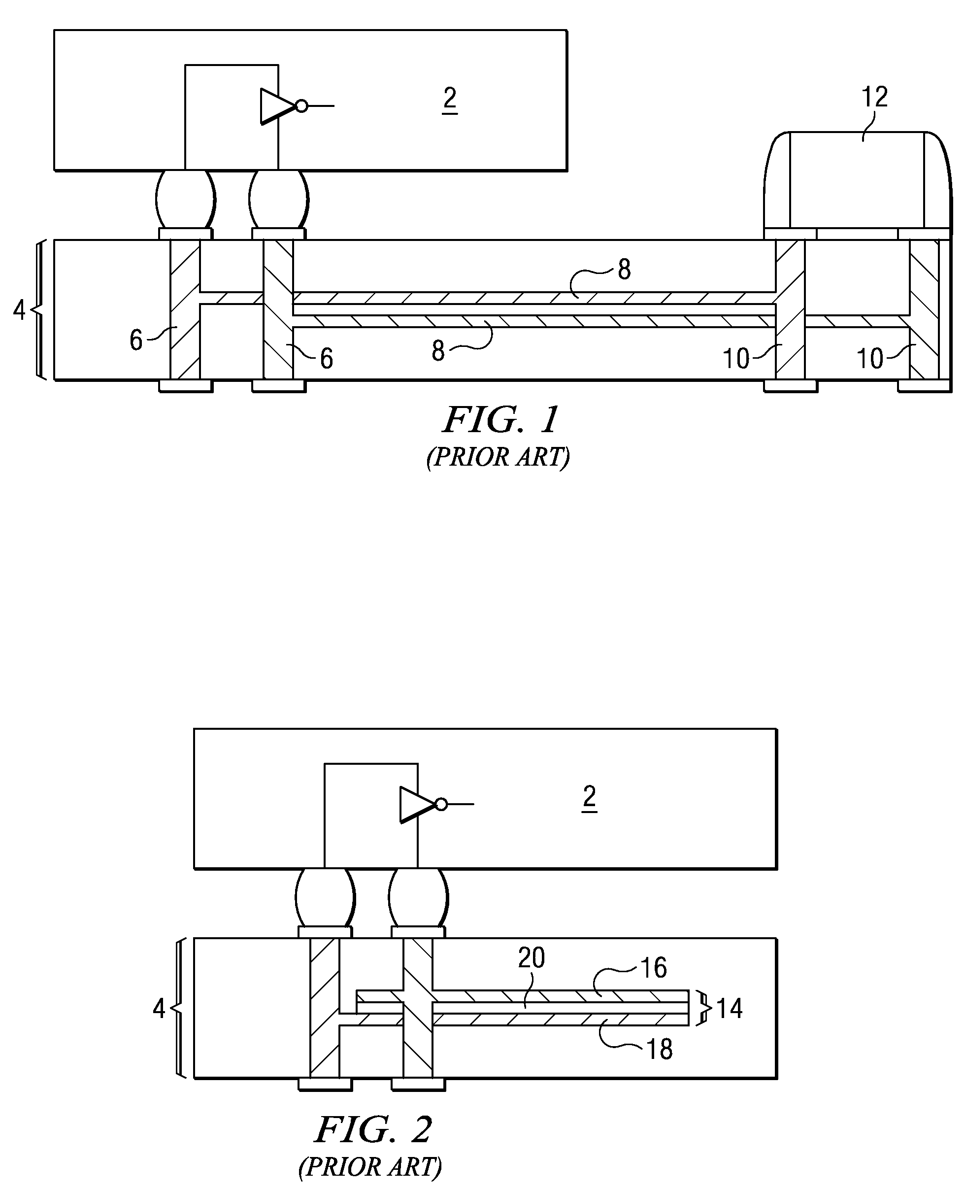
The resonance modes of a parallel-plate waveguide as equivalent for the typical substrate structure can be excited by SSN and cause serious signal integrity and electromagnetic interference problems.
Since the surface-mount capacitor 12 is usually spaced far away from the semiconductor chip 2, it has an inferior ability to suppress the SSN due to the large loop inductance.
However, it is very hard to find and process such materials.
Even if such materials are available, the electrical performances of these materials are often not satisfactory.
However, the stop-bands of the resulting embedded capacitors do not have the central frequencies and bandwidths great enough for the high-frequency applications.

Method used


Image

  • Capacitors with insulating layer having embedded dielectric rods
  • Capacitors with insulating layer having embedded dielectric rods
  • Capacitors with insulating layer having embedded dielectric rods

Examples


Embodiment Construction

[0023]The making and using of the presently preferred embodiments are discussed in details below. It should be appreciated, however, that the present invention provides many applicable inventive concepts that can be embodied in a wide variety of specific contexts. The specific embodiments discussed are merely illustrative of specific ways to make and use the invention, and do not limit the scope of the present invention.

[0024]A novel capacitor and the methods of forming the same structure are presented. Throughout the various views and illustrative embodiments of the present invention, like the reference numbers are used to designate like the elements.

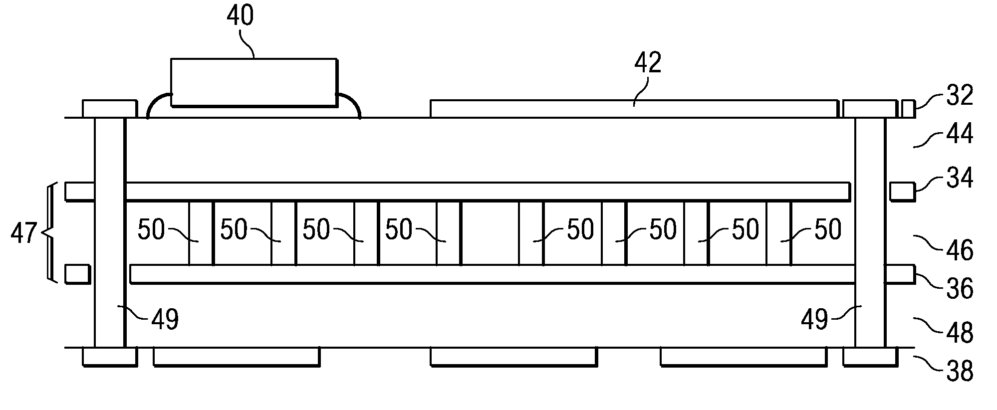
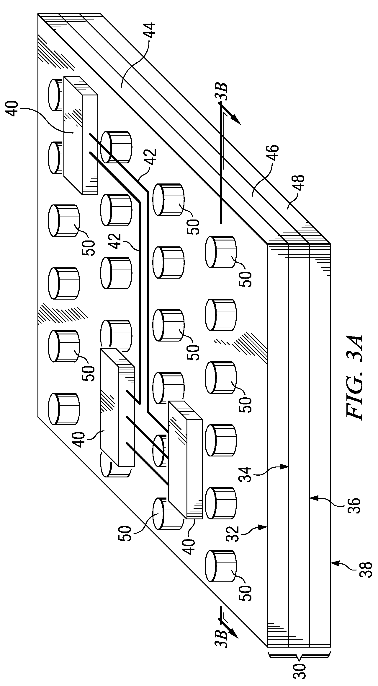
[0025]FIG. 3A illustrates a perspective view of an embodiment of printed circuit board (PCB) 30. In an exemplary embodiment, PCB 30 includes the signal layer 32, power layer 34, ground layer 36, and signal layer 38. As is known in the art, the signal layers 32 and 38 are used to route the electrical connections, while the power layer 3...


PUM


Abstract

A circuit structure is provided. The circuit structure includes a capacitor including a top capacitor electrode; a bottom capacitor electrode parallel to the top capacitor electrode; and an insulating layer between the top and the bottom capacitor electrodes. The insulating layer includes a dielectric rod enclosed by a dielectric material. The dielectric rod has a higher dielectric constant than that of the dielectric material. The circuit structure may be a printed circuit board or packaging substrate, wherein the capacitor is formed between the two layers of the capacitor. Additional dielectric rods may be formed in the insulating layer of the capacitor and spaced apart from the dielectric rods.

Description

TECHNICAL FIELD[0001]This invention relates generally to the decoupling capacitors, and more particularly to the capacitors embedded in the substrate or printed circuit boards.BACKGROUND[0002]High-speed integrated circuits often require the capacitors having a great capacitance density. For example, the bypass capacitors are often used for the reserving power and the decoupling capacitors are used to filter the fluctuating noises. Due to the small sizes of semiconductor chips, the capacitors embedded in the semiconductor dies can only have the large capacitances within the constrained area, often far smaller than required.[0003]To increase the capacitance density of capacitors, discrete surface-mount capacitors were used, as illustrated in FIG. 1. The semiconductor chip 2 is electrically connected to the packaging substrate 4, which includes the plated vias 6. Through the routing metal traces 8, the semiconductor chip 2 is electrically connected to the vias 10, and further to the su...

Claims


Application Information

Patent Timeline
Patent Type & Authority Patents(United States)
IPC IPC(8): H05K1/18
CPCH05K1/162H05K2201/0187H05K2201/09309
Inventor HSU, KUO-CHING STEVENLIN, CHIEN-MINWU, TZONG-LINWU, GUAN-TZONG
Owner TAIWAN SEMICON MFG CO LTD
Learn More